 admin
admin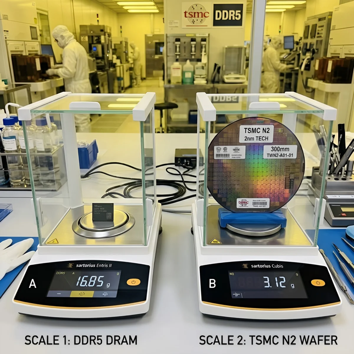
The global semiconductor industry is currently witnessing a historical economic anomaly that underscores the unprecedented demand for memory fueled by the artificial intelligence buildout. In a striking shift in market dynamics, the cost of 1b DRAM per square millimeter has officially surpassed the price of a similar-sized wafer produced on TSMC’s cutting-edge N2 (2-nanometer) node. This development is particularly noteworthy because the N2 process is widely considered the pinnacle of modern lithography, involving significantly more complex fabrication steps, including the transition to Gate-All-Around (GAA) transistor architecture. Despite the immense technical hurdles associated with 2nm logic production, the market value of high-density memory has reached a point where "commodity" silicon is fetching a higher premium than the world’s most advanced logic silicon.
The Mathematical Breakdown of the Pricing Disparity
To understand the scale of this pricing inversion, one must examine the per-wafer and per-area costs associated with the industry’s most advanced nodes. Recent industry data provided by Kernel Insight and corroborated by market analysts indicates that a standard 300mm wafer produced on TSMC’s N3 (3-nanometer) node currently commands a price of approximately $20,000. As the industry transitions to the N2 node, the cost per wafer is projected to rise to roughly $30,000.
When these figures are translated to a per-square-millimeter basis—the standard metric for comparing silicon efficiency—the N3 node costs approximately $0.283 per square millimeter. The more advanced N2 node, despite its $30,000 price tag, results in a cost of approximately $0.424 per square millimeter.
In contrast, the 1b (1-beta) DRAM node, which represents the current state-of-the-art in memory density, presents a much higher cost profile for buyers. The 1b DRAM process features a bit density of roughly 0.436 Gb per square millimeter. With current market reference prices for high-performance memory hovering around $1.50 per Gb, the cost of 1b DRAM reaches approximately $0.654 per square millimeter. This represents a 54 percent premium over TSMC’s N2 logic silicon. Even older generations of memory, such as the 1z DRAM node, are now approaching price parity with N2 logic, with a bit density of 0.273 Gb per square millimeter equating to a cost of $0.410 per square millimeter.
Market Forces and the AI-Driven Supply Crunch
The primary driver behind this price surge is the "chronic shortage" of high-bandwidth and high-density memory. While logic processors like NVIDIA’s H100 or Blackwell series often dominate headlines, these chips are functionally tethered to the availability of DRAM. The rise of Large Language Models (LLMs) has necessitated a massive increase in memory capacity and bandwidth, leading to a "gold rush" for DDR5 and HBM (High Bandwidth Memory) modules.
Industry analysts note that while TSMC’s N2 node is significantly more difficult to fabricate due to the precision required for 2nm features and the implementation of backside power delivery, the pricing is governed by different economic rules. TSMC’s pricing is often based on long-term contracts with a handful of "alpha" customers like Apple, NVIDIA, and AMD. DRAM pricing, however, is more susceptible to spot market fluctuations and the collective purchasing power of hyperscalers like Microsoft, Google, and Meta, who are currently prioritizing inventory accumulation over price sensitivity.
On September 21, 2026, DRAM Exchange reported that 16 Gb DDR5 eTT modules were trading at $24.80, which translates to $1.55 per Gb. This real-world data confirms that the $1.50 reference price used for market analysis is a conservative estimate, suggesting the actual price gap between DRAM and advanced logic may be even wider in specific high-demand sectors.
The Chronology of DRAM Scaling and the Path to 1b
The journey to the 1b node has been marked by incremental but increasingly difficult technological leaps. The industry typically categorizes DRAM generations using alphabet-based nomenclature:

- 1x (10nm-class): The first major step into the sub-20nm era.
- 1y: Refinements in cell capacitor structures.
- 1z: The introduction of more complex multi-patterning techniques.
- 1a (1-alpha): The first node to see limited use of Extreme Ultraviolet (EUV) lithography by some manufacturers.
- 1b (1-beta): The current high-volume frontier, maximizing bit density without yet moving to full 3D DRAM structures.
The 1b node is critical because it represents the limit of what can be achieved with current planar (2D) DRAM architectures before the industry must transition to more radical designs. Manufacturers like Micron, SK Hynix, and Samsung have had to employ sophisticated materials science to maintain capacitor capacitance as the physical space for those capacitors shrinks. This technical wall has limited the number of players capable of producing 1b DRAM at scale, further constricting supply and driving up costs.
Strategic Responses from the "Big Three" and Emerging Players
The current pricing environment has prompted varied strategic responses from the world’s leading memory manufacturers. Samsung Electronics, the world’s largest memory maker, has recently revised its roadmap for the next generation of DRAM, known as "D0a" or "B1b." In a significant shift, Samsung is pulling forward the implementation of hybrid bonding.
Hybrid bonding is a process where the memory cells and the underlying driver circuitry (the "peri") are fabricated on separate wafers and then bonded together. This allows for the stacking of memory cells directly on top of the logic, essentially moving toward a 3D DRAM architecture. While this increases density and performance, the manufacturing cost of hybrid bonding is substantially higher than traditional methods. Samsung’s decision to accelerate this technology suggests that the company expects high DRAM prices to persist, justifying the investment in more expensive fabrication techniques.
Simultaneously, Chinese manufacturers are attempting to close the gap. ChangXin Memory Technologies (CXMT) is reportedly scaling up its G4 and G5 production. CXMT’s G5 product is positioned to compete directly with the Big Three’s 1b and 1c products. If CXMT can successfully scale these nodes, it may provide the market with the necessary supply to normalize prices, although geopolitical trade restrictions and yield challenges remain significant hurdles for the firm.
Technical Complexity vs. Economic Value
The paradox of a "simpler" product costing more than a "complex" one challenges traditional manufacturing logic. TSMC’s N2 node requires the world’s most advanced EUV machines, cleanrooms with near-zero particulate counts, and a supply chain of specialized gases and chemicals that are often single-sourced. The fabrication of a 2nm chip involves hundreds of individual steps, many of which have no margin for error.
DDR5 fabrication, by comparison, is less lithographically intense. However, DRAM requires a unique "tall and thin" capacitor structure that logic chips do not. As nodes shrink, these capacitors become increasingly unstable and difficult to charge. The economic value of 1b DRAM is not derived solely from the cost of the tools used to make it, but from its scarcity in an era where data centers are being built at a record pace. For an AI server, the inability to source 1b DRAM is just as catastrophic as the inability to source an N2-based processor; without the memory, the processor has no data to process.
Broader Implications for the Tech Industry
The fact that DRAM now costs 54 percent more per square millimeter than N2 silicon has profound implications for the hardware ecosystem:
- Increased Bill of Materials (BOM): For device manufacturers, the memory sub-system is becoming the most expensive component of the motherboard. This will likely lead to higher consumer prices for high-end PCs, servers, and mobile devices.
- Investment in 3D DRAM: The high ASP (Average Selling Price) provides a financial cushion for R&D into 3D DRAM. With prices at these levels, the high cost of hybrid bonding and wafer stacking becomes commercially viable.
- TSMC Pricing Pressure: Seeing commodity memory fetch such high premiums may embolden TSMC to further raise its wafer prices. If the market is willing to pay $0.65 per mm² for memory, TSMC may argue that its $0.42 per mm² logic is undervalued.
- Incentive for Efficiency: Software developers may face increased pressure to optimize code for lower memory footprints, as the cost of "throwing more RAM at the problem" becomes prohibitively expensive.
Conclusion
The current pricing trajectory of 1b DRAM serves as a stark reminder of the volatility and interconnectedness of the semiconductor supply chain. While the industry has historically viewed logic as the "brain" and memory as the "commodity," the AI era has leveled the playing field—at least in terms of economic value. As Samsung, Micron, and SK Hynix race to implement hybrid bonding and 3D architectures, and as TSMC prepares for the mass production of N2, the industry is entering a phase where the physical limits of silicon are being matched by the economic limits of the market. For the foreseeable future, the "craziness" of the contemporary AI buildout age shows no signs of abating, ensuring that even the smallest square millimeter of silicon remains some of the most valuable real estate on the planet.