 admin
admin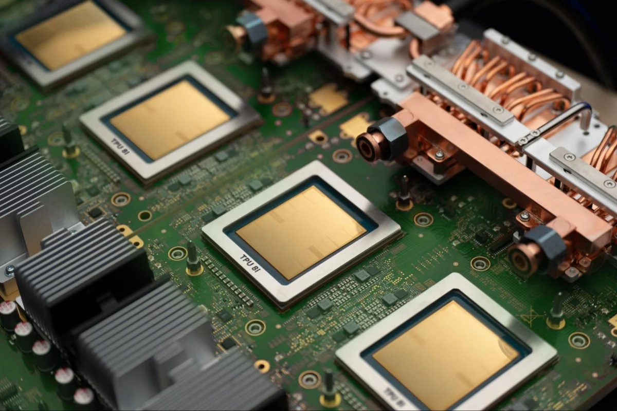
The global race for artificial intelligence supremacy has evolved beyond software algorithms into a high-stakes battle for semiconductor dominance, where the world’s largest technology firms are increasingly seeking to decouple themselves from the supply chain bottlenecks associated with third-party hardware. Google, a pioneer in custom AI silicon through its Tensor Processing Unit (TPU) program, is reportedly preparing a radical architectural shift with its upcoming "Frozen V2" chip. According to a detailed analysis from Morgan Stanley, Google is exploring a design that places static random-access memory (SRAM) directly onto the silicon die, a move intended to optimize the hardware specifically for its Gemini large language models (LLMs) while simultaneously eliminating the need for advanced packaging technologies like TSMC’s Chip-on-Wafer-on-Substrate (CoWoS).
This strategic maneuver represents a fundamental change in how high-performance AI chips are conceived. For years, the industry has relied on the modular assembly of compute logic and high-bandwidth memory (HBM) via sophisticated packaging. However, as demand for NVIDIA’s H100 and B200 GPUs has surged, the packaging stage—specifically TSMC’s CoWoS—has become one of the most significant bottlenecks in the global electronics supply chain. By designing a chip that bypasses this requirement, Google aims to secure a more predictable production roadmap, reduce manufacturing costs, and achieve a level of power efficiency that general-purpose GPUs cannot match.
The Architectural Evolution of Google’s Tensor Processing Units
Google’s journey into custom silicon began over a decade ago when the company realized that the computational requirements of voice recognition and image search would eventually exceed the capacity of traditional CPUs and GPUs. The first TPU, introduced in 2016, was an application-specific integrated circuit (ASIC) designed specifically for AI inference. Since then, the TPU lineage has progressed through multiple iterations, with the TPU v5p and v6 being the most recent benchmarks in AI training and inference at scale.
The reported "Frozen V2" represents a departure from the traditional evolutionary path. In previous generations, Google utilized HBM to handle the massive data throughput required by modern neural networks. HBM requires advanced packaging because the memory stacks are placed alongside the processor on an intermediary layer called an interposer. The Frozen V2 concept suggests a "hardwired" approach. By placing the memory—specifically SRAM—directly on the silicon, Google is attempting to solve the "memory wall" problem, where the speed of data transfer between the processor and memory lags behind the processor’s actual calculation speed.
This integration is tailored specifically to the Gemini architecture. By "freezing" certain elements of the model’s weights or data paths into the silicon layout, Google can minimize the energy-intensive process of moving data across a circuit board or even across a package. This specialization allows for a massive leap in performance-per-watt, a metric that is becoming the primary constraint for modern data centers.
Bypassing the CoWoS Bottleneck and the Role of TSMC
The semiconductor industry is currently facing a supply-demand imbalance in "back-end" manufacturing. While companies like TSMC can manufacture the 5nm or 3nm silicon wafers with relative efficiency, the process of attaching HBM to those wafers using CoWoS is slow and capital-intensive. NVIDIA, the current market leader, is heavily dependent on CoWoS for its high-end AI accelerators, leading to lead times that have, at times, stretched to nearly a year.

Google’s interest in eliminating the packaging step is a calculated move toward supply chain independence. If the Frozen V2 can function effectively without CoWoS, Google can utilize a wider range of fabrication facilities and reduce its reliance on the most constrained segments of TSMC’s production lines.
Industry analysts note that while TSMC remains the likely foundry for the base silicon, the removal of CoWoS changes the economic equation. Packaging typically accounts for a significant portion of the total cost of a high-end AI chip. By simplifying the physical structure of the TPU, Google can potentially lower the per-unit cost of its infrastructure, allowing it to offer Gemini-powered services at a lower price point than competitors who rely on expensive, off-the-shelf hardware.
Strategic Partnerships: Marvell, MediaTek, and Intel
The development of a chip as complex as the Frozen V2 does not happen in a vacuum. Google has a long history of partnering with established semiconductor firms to bring its designs to fruition. Broadcom has traditionally been Google’s primary partner for TPU development, providing the critical intellectual property (IP) and design services required for high-speed networking and memory interfaces.
However, the Morgan Stanley report highlights a potential shift or expansion in Google’s partnership ecosystem. Marvell Technology has emerged as a likely candidate for the Frozen V2 project. Marvell has significant expertise in custom ASIC design and high-speed data interconnects, making them a logical choice for a project that requires deep integration of memory and logic.
Furthermore, rumors have persisted regarding Google’s collaboration with MediaTek and Intel. While high-performance chips typically favor TSMC’s processes, Google is reportedly considering Intel’s EMIB (Embedded Multi-die Interconnect Bridge) technology for its mid-tier or specialized AI accelerators. The choice between Intel’s packaging and a "packaging-free" SRAM approach likely depends on the specific use case: training massive models versus high-speed, low-latency inference. The Frozen V2 appears to be the tip of the spear for the latter, focusing on the efficiency of running Gemini models in real-time.
The Taalas Influence: Hardwiring the Neural Network
The concept of hardwiring an AI model into silicon is not entirely unique to Google. Earlier this year, the startup Taalas gained attention for its approach to "computational logic" that replaces traditional software-programmable processors with fixed-function silicon.
In a traditional GPU, the hardware is flexible; it can run any model, from a simple linear regression to a complex transformer, by loading different software instructions. The downside of this flexibility is overhead—energy is wasted on instruction fetching, decoding, and managing a generic memory hierarchy. Taalas, and now Google with Frozen V2, are moving toward a paradigm where the silicon is the model.

By hardwiring the weights and the structure of the Gemini neural network into the silicon, Google effectively turns the chip into a physical manifestation of the AI. This results in speeds that are orders of magnitude faster than programmable chips, but it comes with a significant trade-off: lack of flexibility. If Google makes a fundamental change to the Gemini architecture, the Frozen V2 chips could become obsolete. However, for a company that controls both the model and the hardware, this "vertical integration" allows for an optimization loop that is unavailable to companies like NVIDIA, which must cater to thousands of different customers with varying needs.
Chronology of Development and Market Entry
The timeline for the Frozen V2 suggests a long-term strategic play rather than an immediate product launch. According to industry projections:
- 2024-2025: Design finalization and early prototyping. Google and its partners (likely Marvell) are expected to refine the SRAM-on-silicon architecture and conduct initial "tape-outs."
- 2026: Early-stage pilot production. This phase will focus on yield optimization. As noted by analysts, moving from a 90% yield to a 98% yield is critical for the economic viability of custom silicon.
- 2027: Limited deployment within Google’s internal data centers. Initial testing of Frozen V2 with Gemini-specific workloads.
- 2028: Broad production ramp. This is the year Google is expected to integrate these chips at scale across its global infrastructure, potentially displacing a significant portion of its remaining third-party GPU fleet.
Implications for the AI Market and Infrastructure
The shift toward model-specific silicon like the Frozen V2 has profound implications for the broader technology landscape. First, it signals the "commoditization" of AI hardware for the largest players. If Amazon (with Trainium), Microsoft (with Maia), and Google (with TPU/Frozen) successfully transition to internal silicon, the total addressable market for NVIDIA’s general-purpose GPUs among "Hyperscalers" may begin to contract.
Second, this move highlights the growing importance of "Inference at the Edge" and "Inference at Scale." As AI moves from a novelty to a core component of every Google product—from Search to Workspace—the cost of running those models becomes a primary business concern. A chip that is 10 times more efficient at running Gemini could save Google billions of dollars in electricity and cooling costs over the lifetime of a data center.
Finally, the move challenges the traditional semiconductor manufacturing model. If the future of AI hardware lies in eliminating packaging and hardwiring logic, the value proposition of the industry may shift away from "packaging specialists" back toward "design and logic specialists."
Conclusion: A High-Stakes Bet on Vertical Integration
Google’s Frozen V2 project is more than just a technical experiment; it is a declaration of independence from the current constraints of the semiconductor industry. By attempting to place SRAM directly on the silicon and bypassing the CoWoS bottleneck, Google is betting that specialization will beat generalization in the long run.
The risks are substantial. The "hardwired" nature of the chip means Google must be certain that the Gemini architecture will remain relevant for years to come. Furthermore, the technical hurdles of managing heat and yield on a massive, SRAM-heavy die are significant. However, if successful, the Frozen V2 could provide Google with a structural advantage in the AI race, allowing it to deliver more powerful AI models with greater efficiency and lower costs than any of its rivals. As the industry moves toward 2028, the success of Frozen V2 will be a key indicator of whether the future of AI belongs to the flexible giants like NVIDIA or the vertically integrated pioneers like Google.