 admin
admin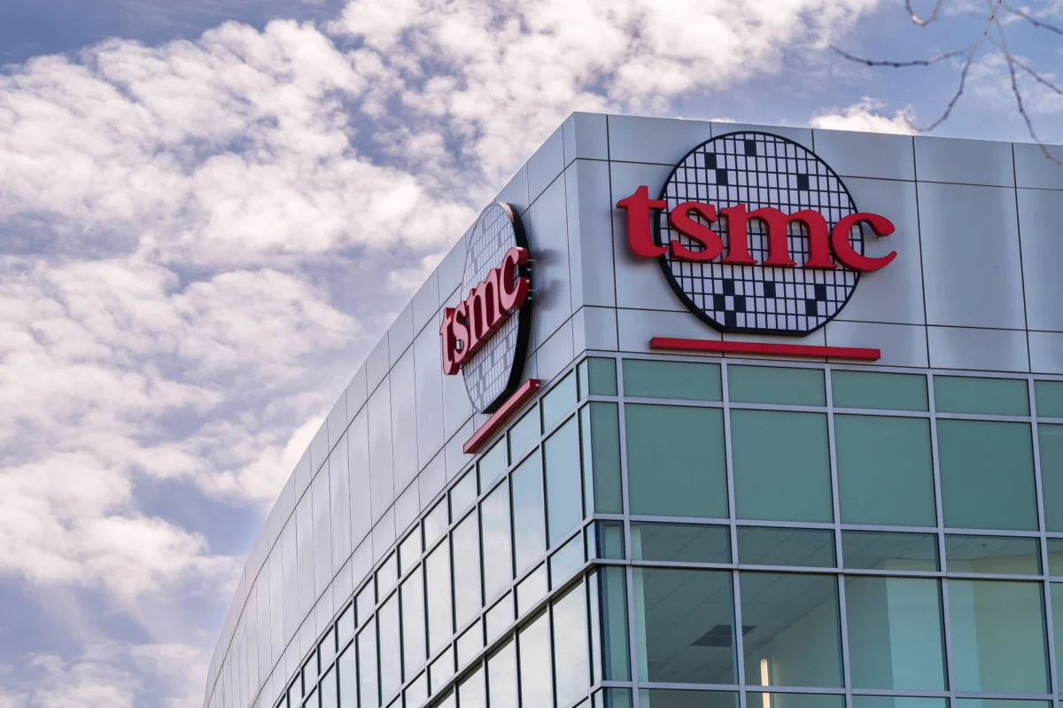
The global semiconductor landscape is currently undergoing a seismic shift as the Taiwan Semiconductor Manufacturing Company (TSMC) prepares to aggressively scale its advanced packaging capabilities. According to recent reports from Taiwanese industry analysts, the world’s leading foundry is poised to double its Chip-on-Wafer-on-Substrate (CoWoS) capacity from its projected 2026 levels by the year 2028. This expansion is driven by the insatiable demand for artificial intelligence (AI) accelerators, primarily from industry titans like NVIDIA and AMD. As the current supply chain struggles to keep pace with the generative AI boom, TSMC’s roadmap suggests a massive capital commitment to maintaining its dominance in the high-end packaging sector, even as competitors like Intel and alternative suppliers like Amkor and UMC ramp up their own offerings.
The Strategic Roadmap: Scaling CoWoS to 260,000 Wafers
The trajectory for TSMC’s CoWoS production is one of exponential growth. Current industry data indicates that by the end of 2024, TSMC’s total CoWoS capacity is expected to reach approximately 130,000 wafers per month. However, the projected demand for AI GPUs—specifically NVIDIA’s Blackwell architecture and subsequent generations—has forced a revision of long-term capacity goals. Analysts now anticipate that TSMC will push its capacity to 260,000 wafers per month by the close of 2028.
This expansion is not merely a matter of adding more machinery to existing floors; it involves the construction and optimization of specialized facilities. Central to this plan is the AP7 facility in Taiwan, which is being designed as a hub for next-generation advanced packaging. Furthermore, the expansion extends beyond Taiwanese borders. TSMC’s Arizona campus in the United States is playing an increasingly critical role. While the Arizona site is currently focused on front-end wafer fabrication (creating the logic chips themselves), the lack of domestic advanced packaging facilities in the U.S. remains a logistical bottleneck. Currently, wafers produced in Arizona must be transported back to Taiwan for CoWoS packaging before they can be integrated into final server systems. The 2028 roadmap suggests a more integrated approach, potentially bringing more back-end processes closer to the front-end production sites to reduce lead times and geopolitical risk.
Technological Architecture: CoWoS vs. Intel’s EMIB-T
To understand why this capacity expansion is so critical, one must examine the technological requirements of modern AI. High-performance GPUs require massive data throughput between the logic processor and High Bandwidth Memory (HBM). Standard packaging techniques are insufficient for these speeds, leading to the development of 2.5D and 3D packaging.
TSMC’s CoWoS technology utilizes a silicon interposer—a middle layer of silicon that sits between the chips and the substrate. This interposer features Through Silicon Vias (TSVs), which are vertical microscopic tunnels that allow for incredibly dense wiring. This density enables high bandwidth and low latency, which are the primary requirements for NVIDIA’s H100 and B200 chips. Without CoWoS, the communication between the GPU and the HBM would become a bottleneck, severely limiting the performance of AI models.
In contrast, Intel has developed its own competing technology known as EMIB-T (Embedded Multi-die Interconnect Bridge). Architecturally, EMIB-T differs significantly from CoWoS. Instead of a full silicon interposer covering the entire area under the chips, EMIB-T uses small silicon "bridges" embedded directly into the organic substrate. This approach is often considered more cost-effective for certain applications because it uses less silicon than a full interposer.

Reports suggest that Intel is making significant strides with EMIB-T. Analysts estimate that Intel’s equivalent capacity for EMIB-T (when converted to the standard 12-inch wafer metric used for CoWoS) will reach 15,000 to 20,000 wafers per month in 2027. By 2028, this is expected to jump to between 40,000 and 45,000 wafers per month. While this remains a fraction of TSMC’s projected 260,000 wafers, it positions Intel as a vital secondary source, particularly for custom silicon projects.
The Rise of Custom AI Silicon and the Spillover Effect
The current shortage of TSMC’s CoWoS capacity has created a "spillover" effect that is reshaping the supplier ecosystem. Major cloud service providers (CSPs) such as Google and Amazon are increasingly designing their own AI chips (TPUs and Trainium/Inferentia) to reduce their dependence on NVIDIA. Because TSMC’s capacity is largely reserved for NVIDIA and AMD, these custom silicon projects are seeking alternatives.
Intel’s EMIB-T has become a primary beneficiary of this trend. Google, for instance, has leveraged Intel’s packaging technology for its latest Tensor Processing Units. The architectural flexibility of EMIB-T makes it highly suitable for these custom designs, which may not require the extreme density of a full silicon interposer but still demand high-speed interconnects.
Furthermore, the capacity crunch at TSMC has provided a windfall for Outsourced Semiconductor Assembly and Test (OSAT) companies. Firms such as Amkor Technology, United Microelectronics Corporation (UMC), and ASE Technology have seen a surge in orders. UMC has been collaborating with partners to offer "CoWoS-like" solutions, providing the silicon interposers while OSATs like Amkor handle the final assembly. This modular approach allows the industry to bypass some of the bottlenecks at TSMC, though TSMC remains the gold standard for the most demanding flagship AI products.
Chronology of the Packaging Crisis and Expansion
The journey to the 2028 capacity targets began in late 2022, following the public release of ChatGPT, which triggered an unprecedented surge in demand for AI compute.
- 2023: TSMC recognized that its existing CoWoS lines were insufficient. Lead times for AI GPUs stretched to over 52 weeks. The company began converting existing logic capacity to packaging space.
- 2024: Capacity reached approximately 130,000 wafers per month. TSMC Chairman C.C. Wei publicly acknowledged that while the company was doubling capacity year-over-year, it was still not enough to satisfy customers.
- 2025-2026: The focus shifts to the "Phase 2" expansion. New facilities in Chiayi, Taiwan, are expected to come online. Intel begins to market its Foundry Services (IFS) more aggressively, offering EMIB-T to external customers.
- 2027: Intel is projected to hit the 20,000-wafer milestone. The industry begins to see the first results of the U.S. CHIPS Act, with advanced packaging facilities starting to break ground on American soil.
- 2028: TSMC hits the 260,000-wafer mark. The market enters a more stabilized phase where supply finally begins to align with the normalized demand of a mature AI industry.
Logistical Challenges and Global Geopolitics
One of the most complex aspects of this expansion is the geographical distribution of the supply chain. Currently, the semiconductor industry is heavily "front-end heavy" in the United States and "back-end heavy" in Taiwan. TSMC’s Arizona fabs are a testament to the push for American-made chips, but without local packaging, the "Made in USA" label is complicated by a round-trip flight across the Pacific.
Shipping wafers to Taiwan for packaging adds costs, increases carbon footprints, and introduces risks related to regional stability. Analysts suggest that for TSMC to truly double its effective capacity by 2028, it must resolve these logistical hurdles. This may involve incentivizing its partners, like Amkor, to build large-scale facilities in close proximity to the Arizona fabs. Amkor has already announced plans for a $2 billion packaging facility in Arizona, which will specifically support Apple and potentially other TSMC customers.

Market Implications and Economic Analysis
The move to double CoWoS capacity reflects a broader belief in the longevity of the AI investment cycle. TSMC’s capital expenditure (CapEx) is a leading indicator for the entire tech sector. By committing to 260,000 wafers per month, TSMC is signaling that it does not view the AI boom as a temporary bubble.
For NVIDIA and AMD, this capacity increase is a lifeline. It allows them to move from a "supply-constrained" model to a "demand-driven" model. For the end-users—the developers of Large Language Models (LLMs)—increased supply should eventually lead to more competitive pricing for compute power, lowering the barrier to entry for AI innovation.
However, the high cost of advanced packaging remains a factor. CoWoS is significantly more expensive than traditional packaging. As TSMC and Intel scale, the industry will be watching to see if economies of scale can bring down the per-wafer cost. If costs remain high, only the wealthiest tech giants will be able to afford the highest-tier AI hardware, potentially centralizing AI power in the hands of a few "Hyperscalers."
Conclusion: A New Era of Semiconductor Manufacturing
The projected doubling of TSMC’s CoWoS capacity by 2028, coupled with Intel’s aggressive expansion of EMIB-T, marks the beginning of the "Packaging Era" in semiconductors. For decades, the industry focused on shrinking transistors (Moore’s Law). Today, the focus has shifted to how those transistors are connected and packaged.
As TSMC targets 260,000 wafers per month, the company is not just building factories; it is building the infrastructure of the future global economy. The success of this expansion will determine the pace of AI advancement for the next decade. While TSMC remains the undisputed leader, the rise of Intel’s packaging services and the growth of OSAT providers like Amkor and ASE ensure a more resilient, albeit still strained, global supply chain. The road to 2028 will be defined by massive capital outlays, technological breakthroughs in 3D stacking, and a continued geopolitical tug-of-war over where these critical components are assembled.