 admin
admin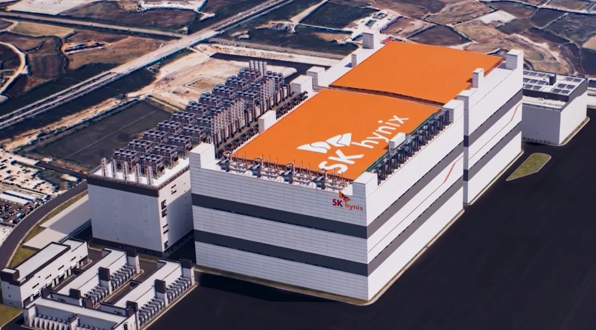
SK Hynix CEO Kwak No-Jung, speaking at the 2026 Global Forum in Santa Clara, California, has outlined a comprehensive roadmap for the company to maintain its dominance in the semiconductor industry through the rapid expansion of global production bases and the deployment of next-generation memory solutions. The forum, held on June 18 at the Santa Clara Marriott Hotel, served as a platform for the South Korean memory giant to signal its intent to lead the artificial intelligence (AI) era by aligning its manufacturing capacity with the skyrocketing demand for high-performance compute hardware. As the AI industry undergoes a paradigm shift toward more complex, multi-modal models, SK Hynix is positioning itself as the indispensable partner for hardware accelerators, emphasizing that the future of AI is fundamentally tethered to the evolution of memory technology.
The 2026 Global Forum comes at a critical juncture for the semiconductor sector. Over the past three years, the explosion of generative AI has transformed memory from a commodity component into a high-value, high-performance bottleneck. SK Hynix, which currently holds a significant lead in the High Bandwidth Memory (HBM) market, is seeking to fortify this position against intensifying competition from Samsung Electronics and Micron Technology. CEO Kwak’s address highlighted a dual-track strategy: the aggressive expansion of physical infrastructure across South Korea and the United States, coupled with a technical roadmap that pushes the boundaries of DRAM density and bandwidth.
Global Production Footprint and Infrastructure Expansion
Central to SK Hynix’s growth strategy is the development of the Yongin Semiconductor Cluster in Gyeonggi Province, South Korea. This massive project represents one of the largest private-sector investments in the nation’s history. The cluster is designed to house four state-of-the-art fabrication plants (fabs) and a dedicated mini-fab for research and development. By centralizing its production and R&D within this cluster, SK Hynix aims to achieve unprecedented economies of scale and accelerate the "lab-to-fab" transition for new memory architectures. The first fab in the Yongin cluster is expected to be a cornerstone for the mass production of next-generation DRAM, providing the necessary volume to meet the needs of global hyperscalers and AI chip designers.
Simultaneously, SK Hynix is making significant inroads into the United States. The company’s planned facility in Indiana marks a strategic pivot toward localized manufacturing in North America. This site will focus on advanced semiconductor packaging, a field that has become increasingly vital as Moore’s Law slows and chiplet-based designs become the industry standard. The Indiana fab is expected to specialize in the stacking and packaging of HBM, placing SK Hynix in close geographical proximity to major U.S.-based clients such as NVIDIA, AMD, and Intel. This move not only mitigates supply chain risks but also aligns with the U.S. government’s initiatives to bolster domestic semiconductor capabilities through the CHIPS and Science Act.
Beyond manufacturing, the establishment of a new global AI research and development center in the United States underscores the company’s commitment to architectural innovation. This center will serve as a hub for collaborating with Silicon Valley’s software and hardware ecosystems, ensuring that SK Hynix’s memory designs are optimized for the specific requirements of next-generation AI algorithms. By integrating R&D efforts across both Korea and the U.S., the company intends to create a feedback loop that informs its technical roadmap with real-world performance data from the world’s leading AI developers.

Technical Roadmap: HBM4, DDR6, and the Shift to HBM4E
The technological core of SK Hynix’s strategy revolves around the transition to HBM4 and beyond. As of 2026, the industry is witnessing the deployment of HBM4 in top-tier AI accelerators, including NVIDIA’s Rubin architecture. HBM4 represents a significant leap over its predecessor, HBM3E, by doubling the interface width from 1024-bit to 2048-bit. This change allows for higher bandwidth at lower clock speeds, which is essential for managing the thermal envelopes of dense AI server racks.
SK Hynix is already sampling HBM4E, the enhanced version of the fourth-generation standard. HBM4E is projected to offer capacities of up to 48GB per stack with speeds reaching 16Gbps per pin. These specifications are critical for training Large Language Models (LLMs) that require massive datasets to be held in close proximity to the processor. The company’s ability to yield these complex 12-layer and 16-layer stacks will likely determine its market share in the 2026-2028 window.
Furthermore, the company is preparing for the transition in the consumer and enterprise PC markets with the development of DDR6 and LPDDR6. While AI servers are the primary revenue drivers, the rise of "AI PCs" and high-end smartphones requires a new generation of system memory. DDR6 is expected to double the data rates of DDR5, while LPDDR6 will focus on providing high bandwidth with ultra-low power consumption, a necessity for on-device AI processing. SK Hynix expects these standards to reach commercialization between late 2026 and 2028, ensuring that its technological superiority extends across the entire computing spectrum.
The Strategic Interdependence of Memory and AI
During his keynote, CEO Kwak No-Jung articulated a vision where memory is the foundational layer of the AI ecosystem. "The artificial intelligence industry cannot exist without memory," Kwak stated, highlighting that the computational power of modern GPUs and TPUs is effectively throttled by the speed at which data can be moved from storage to the processing cores. This "memory wall" has become the primary challenge for AI engineers.
SK Hynix’s response to this challenge involves moving beyond traditional memory roles. The company is exploring Processing-in-Memory (PIM) and Computational Storage, where basic logic functions are integrated directly into the memory chips. This reduces the need to move data back and forth across the system bus, significantly lowering power consumption—a critical factor for data centers facing strict energy constraints. By evolving from a component supplier to a systems-solution provider, SK Hynix aims to capture a larger portion of the AI value chain.
Competitive Dynamics and Market Pressures
The memory market remains a fierce three-way race between SK Hynix, Samsung, and Micron. While SK Hynix currently enjoys a "first-mover" advantage in HBM, Samsung has pledged massive investments to reclaim its top spot, leveraging its foundry capabilities to offer integrated logic-and-memory solutions. Micron, meanwhile, has made significant strides in power efficiency with its HBM3E offerings, securing a portion of NVIDIA’s supply chain.

Adding to the competitive pressure is the rapid rise of Chinese manufacturers, most notably ChangXin Memory Technologies (CXMT). Driven by domestic demand and heavy state subsidies, CXMT has seen its revenue explode as it gains share in the standard DRAM market. While Chinese firms currently lag in high-end HBM production, their aggressive expansion in legacy and mid-range memory segments could force the "Big Three" to accelerate their exit from lower-margin products and double down on advanced AI memory.
SK Hynix’s strategy of building global production bases is, in part, a defensive move against these shifting market dynamics. By establishing high-end packaging in the U.S. and a massive, efficient cluster in Korea, the company is creating a moat based on technical complexity and geographical diversification that newer entrants will find difficult to replicate.
Organizational Philosophy: The "One-Team" Culture
A notable aspect of Kwak’s presentation was the emphasis on SK Hynix’s "One-Team" culture. This internal philosophy focuses on breaking down silos between design, process engineering, and packaging departments. In the era of HBM, where the boundary between a memory chip and a logic chip is blurring, this interdisciplinary collaboration is vital. The "One-Team" approach extends to external partnerships as well. SK Hynix has fostered deep "co-engineering" relationships with key equipment suppliers and foundry partners like TSMC to ensure that its HBM stacks are perfectly compatible with the world’s most advanced logic processes.
Broader Impact and Industry Implications
The implications of SK Hynix’s 2026 roadmap extend far beyond the company’s balance sheet. The massive capital expenditure required for the Yongin and Indiana projects will stimulate the global semiconductor equipment market, benefiting companies like ASML, Applied Materials, and Tokyo Electron. Furthermore, the successful rollout of HBM4 and HBM4E will dictate the pace of AI advancement. If memory bandwidth continues to scale, AI developers can build even larger and more capable models. Conversely, any supply constraints in the memory sector could lead to a slowdown in the deployment of AI infrastructure globally.
As the industry moves toward 2027 and 2028, the semiconductor landscape will likely be defined by how well companies can integrate into the AI-centric economy. SK Hynix’s proactive stance—securing land, talent, and technology years in advance—reflects a recognition that the "memory boom" is not a temporary cycle but a fundamental restructuring of the industry. By the time the Yongin and Indiana facilities reach full capacity, SK Hynix intends to have transitioned from a traditional DRAM maker into the premier architect of the AI era’s most vital resource.