 admin
admin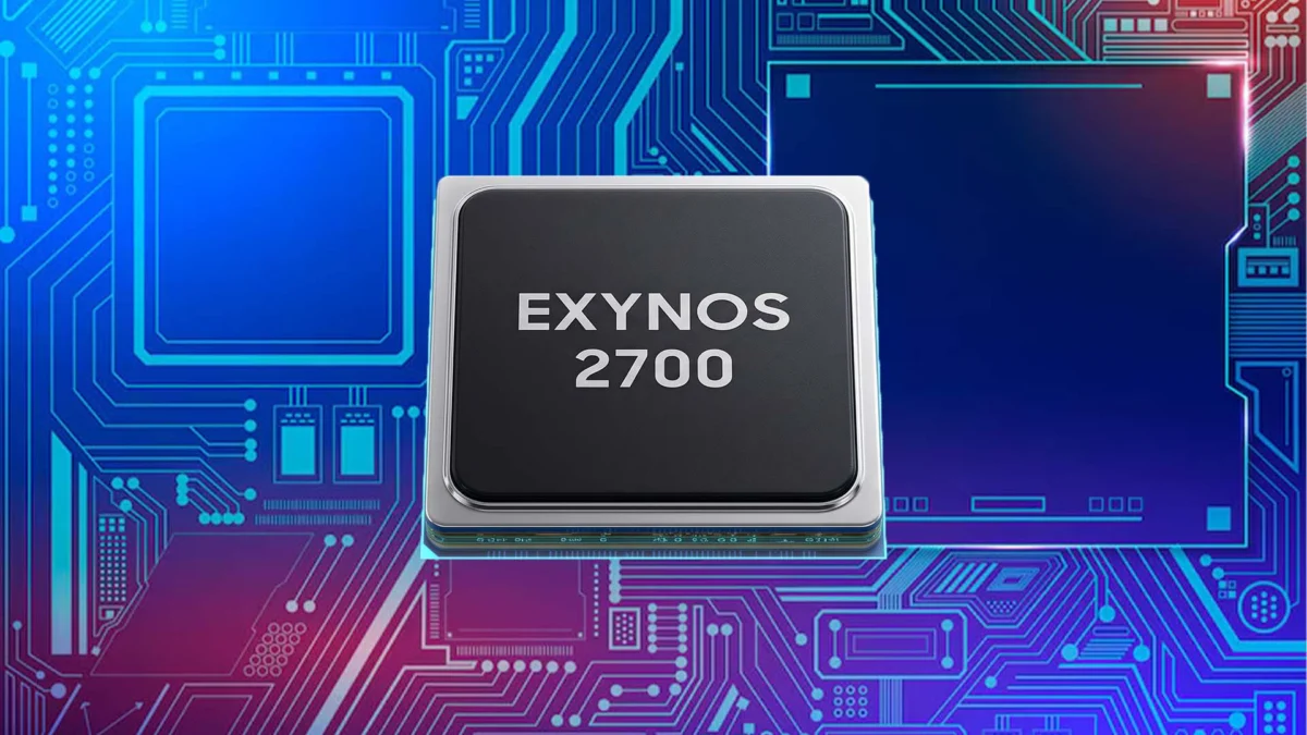
Samsung Electronics has officially confirmed that the development of its upcoming flagship mobile processor, the Exynos 2700, is proceeding according to internal timelines without significant technical setbacks. This announcement signals a pivotal moment for the South Korean conglomerate’s semiconductor division, Samsung Foundry, as it prepares to deploy its second-generation 2nm Gate-All-Around (GAA) process, known as the SF2P node. Industry insiders and technical analysts suggest that if Samsung successfully stabilizes this node and achieves its projected yield targets, the Exynos 2700 could become the first mobile chipset in the company’s history to break the 4.00GHz clock speed barrier, potentially reaching a peak frequency of 4.20GHz.
The transition to the SF2P node represents more than just a marginal improvement over the standard SF2 process. It is a refined, performance-oriented iteration designed specifically to address the thermal and efficiency challenges that have historically hampered the Exynos line. As the global smartphone market shifts toward on-device generative artificial intelligence (AI) and high-fidelity mobile gaming, the demand for sustained high-frequency performance has never been greater. For Samsung, the Exynos 2700 is not merely a component for its future Galaxy S27 series; it is a critical demonstration of its ability to compete with TSMC’s 2nm offerings and Qualcomm’s Snapdragon Elite series.
The Evolution of Samsung’s 2nm GAA Roadmap
The roadmap for Samsung’s 2nm journey began with the initial announcement of its Gate-All-Around (GAA) architecture, a departure from the traditional FinFET (Fin Field-Effect Transistor) design. GAA technology allows for more precise control over current flow by surrounding the channel with the gate on all four sides. This reduces current leakage and improves power efficiency—factors that are vital when pushing silicon toward the 4.00GHz threshold.
Samsung’s 2nm strategy is divided into several phases. The initial SF2 node is designed for general-purpose high-performance computing, while the SF2P (Performance) node is a specialized version optimized for higher clock speeds and better power-to-performance ratios. The Exynos 2600, which precedes the 2700, is expected to utilize the earlier iterations of this 2nm process. While the Exynos 2600 is rumored to reach a maximum clock speed of 3.90GHz, it has reportedly faced challenges regarding power draw, with some benchmarks indicating peak consumption as high as 30W.
By the time the Exynos 2700 enters mass production in the second half of 2026, Samsung intends to have matured the SF2P node to a point where manufacturing consistency can support higher frequencies without the catastrophic thermal throttling seen in previous generations. This maturation is a prerequisite for the Exynos 2700 to transition from a "burst performance" chip to a "sustained performance" powerhouse.
The Physics of Yields and Manufacturing Consistency
A critical factor in the success of the Exynos 2700 is the yield rate—the percentage of functional chips produced from a single silicon wafer. According to industry analyst reports, Samsung achieved approximately 60 percent yields on its initial 2nm GAA process. For the Exynos 2700 to be commercially viable and hit its performance targets, projections from sources such as @phonefuturist suggest that Samsung must push SF2P yields into the 65-70 percent range by late 2026.

The relationship between yield and performance is rooted in semiconductor physics. Higher yields indicate a high degree of manufacturing stability, where transistors switch cleanly and signal travel delays (RC delay) are minimized. When yields are low, it often indicates "dirty" switching or significant current leakage. In such scenarios, increasing the voltage to achieve higher clock speeds results in exponential increases in heat. Conversely, with a 70 percent yield, the "silicon lottery" favors the manufacturer, providing more chips that can operate at 4.20GHz within a safe thermal envelope.
The targeted 4.20GHz prime core frequency for the Exynos 2700 will inevitably require a voltage increase compared to the Exynos 2600. However, if the SF2P node delivers the promised reduction in current leakage, the thermal headroom created will allow the chip to maintain these high speeds for longer durations. This is essential for modern workloads, such as real-time AI image processing and 8K video encoding, which require the CPU to remain in a high-power state without triggering immediate performance down-clocking.
Architectural Shifts: Moving Toward Side-by-Side Packaging
Beyond the lithography of the chip itself, Samsung is reportedly overhauling the physical architecture of the Exynos 2700. Traditionally, mobile SoCs (System-on-Chips) have utilized "on-package" memory, where the RAM is stacked directly on top of the processor. While this saves space, it creates a "heat sandwich" effect, where the heat from the CPU and the heat from the RAM exacerbate one another, leading to rapid thermal saturation.
For the Exynos 2700, Samsung is expected to move away from this traditional PoP (Package-on-Package) approach in favor of a Side-by-Side (SbS) architecture. This method is similar to Apple’s A20 Pro WMCM (Wafer-Level Multi-Chip Module) design. By placing the memory modules adjacent to the processor rather than directly on top of them, Samsung can significantly improve the heat dissipation surface area.
This SbS architecture, combined with a "Heat Pass Block" (HPB) approach, could revolutionize the thermal profile of the Exynos series. Internal Samsung data suggests that the Heat Pass Block is exceptionally effective at moving heat away from the core logic, with some hyperbolic internal comparisons suggesting efficiency levels that rival extreme cooling methods like liquid nitrogen in specific laboratory conditions. While real-world applications will be more modest, the combination of a 2nm SF2P node and SbS packaging represents a multi-pronged attack on the thermal issues that have plagued the Exynos brand for years.
Chronology of Development and Market Context
To understand the stakes for the Exynos 2700, one must look at the timeline of Samsung’s recent foundry performance:
- 2021-2022: Samsung struggles with 4nm yields, leading to the "GOS (Game Optimization Service) scandal" where Galaxy S22 devices were throttled to prevent overheating.
- 2023: Samsung skips the Exynos 2300 in favor of a global Snapdragon-only strategy for the Galaxy S23, allowing time to reset its foundry goals.
- 2024: The Exynos 2400 debuts with the Galaxy S24, showing significant improvements in stability and narrow performance gaps with Qualcomm.
- 2025 (Projected): The Exynos 2500 is expected to utilize the 3nm GAA process, acting as a bridge to the 2nm era.
- 2026 (Projected): The Exynos 2600 introduces the first-generation 2nm node, aiming for 3.90GHz.
- Late 2026/Early 2027: The Exynos 2700 launches on the SF2P node, targeting the 4.20GHz milestone.
This chronology demonstrates a gradual but determined effort by Samsung to reclaim its status as a premier chip designer. The Exynos 2700 is positioned as the culmination of this five-year recovery plan.

Industry Implications and Competitive Landscape
The success of the Exynos 2700 will have ripple effects across the entire technology industry. For Samsung’s mobile division (MX Business), a high-performing Exynos chip provides critical leverage in price negotiations with Qualcomm. Historically, when the Exynos chip underperforms, Samsung is forced to pay a premium for Snapdragon processors, which impacts the profit margins of the Galaxy S series.
From a broader market perspective, the Exynos 2700 will be competing directly with Apple’s A20 or A21 Pro and Qualcomm’s Snapdragon 8 Gen 6 or Gen 7. Apple has traditionally led the industry in single-core performance, but the gap has narrowed. If Samsung can deliver a 4.20GHz prime core with sustained thermal stability, it could feasibly match or exceed the single-core performance of its rivals, a feat the company has not achieved in over half a decade.
Furthermore, the advancement of the SF2P node is vital for Samsung Foundry’s contract manufacturing business. Potential clients, such as NVIDIA or Tesla, watch the performance of Samsung’s internal chips as a bellwether for the foundry’s capabilities. A successful Exynos 2700 would serve as a powerful marketing tool to lure "fabless" semiconductor companies back to Samsung and away from TSMC’s near-monopoly on high-end nodes.
Conclusion: Sustained Performance over Peak Metrics
While the 4.20GHz clock speed is a headline-grabbing figure, technical analysts emphasize that the true measure of the Exynos 2700’s success will be its efficiency curve. The mobile industry is moving away from judging chips based on short-burst benchmark scores like Geekbench 6. Instead, the focus is shifting toward "performance per watt" and the ability to maintain high clock speeds during extended gaming sessions or complex AI workloads.
Samsung’s decision to integrate Heat Pass Block technology and Side-by-Side packaging suggests that the company is finally prioritizing the thermal bottleneck. If the Exynos 2700 can deliver a 4.00GHz+ experience that does not result in the 30W power spikes seen in early 2nm testing, it will mark a successful transition into the next era of mobile computing. For consumers, this could mean a Galaxy S27 that offers desktop-class processing power with the battery life and thermal comfort required for a handheld device. As the second half of 2026 approaches, the industry remains cautiously optimistic that Samsung’s "no setbacks" claim will translate into a product that finally redeems the Exynos brand.