 admin
admin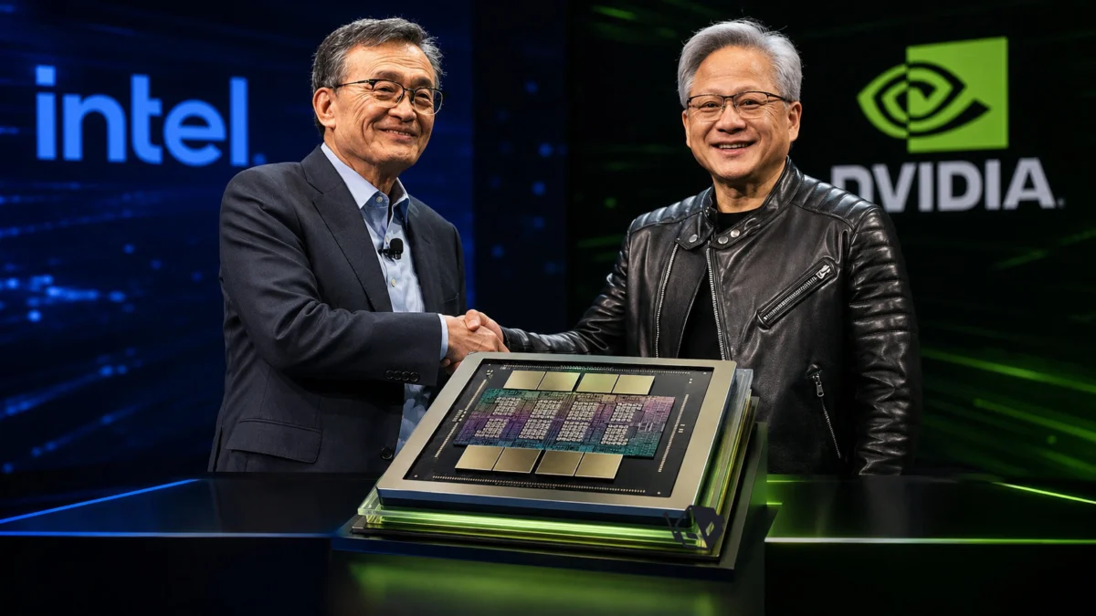
Intel’s strategic pivot toward becoming a world-class semiconductor foundry has reached a significant milestone with reports indicating a major partnership with NVIDIA for its upcoming "Feynman" GPU architecture. This collaboration is expected to see Intel Foundry provide both advanced wafer fabrication and sophisticated packaging solutions for NVIDIA’s next-generation AI accelerators, slated for a 2028 release. The deal represents a fundamental shift in the semiconductor landscape, as NVIDIA, the world’s leading AI chip designer, looks to diversify its supply chain and leverage Intel’s aggressive roadmap in the Angstrom era of process technology.
The partnership centers on the Feynman GPU, which is positioned as the successor to the Rubin architecture. According to industry insiders and recent financial disclosures, Intel is slated to utilize its 14A (1.4nm-class) process node and EMIB-T (Embedded Multi-die Interconnect Bridge) packaging technology to meet NVIDIA’s rigorous performance and density requirements. This development follows months of speculation regarding NVIDIA’s interest in Intel’s "IDM 2.0" strategy, which opened Intel’s manufacturing doors to external customers, including direct competitors.
Historical Context and the Road to Collaboration
The relationship between Intel and NVIDIA has evolved from one of pure competition to a complex, symbiotic partnership. Historically, Intel dominated the data center with its Xeon processors, while NVIDIA focused on discrete GPUs. However, the explosion of generative AI necessitated a closer integration of CPU and GPU resources.

Earlier in 2024, reports surfaced that NVIDIA was evaluating Intel’s 18A and 14A process nodes. This interest was driven by two primary factors: the need for geographic diversification of manufacturing and the immense capacity constraints currently facing the Taiwan Semiconductor Manufacturing Company (TSMC). While TSMC remains NVIDIA’s primary partner, the sheer volume of demand for AI hardware has forced NVIDIA to seek "secondary" sources that can offer comparable technical sophisticated.
Intel’s recent Q2 2026 earnings call provided further evidence of this momentum. Leadership emphasized a disciplined but aggressive increase in Capital Expenditure (CapEx) specifically targeted at advanced packaging and front-end fabrication. This investment is backed by long-term customer agreements, which analysts believe include high-stakes contracts with NVIDIA. The leadership transition and the infusion of industry veterans into Intel’s Foundry division have been cited as key drivers in securing these high-profile design wins.
Technical Analysis of the Feynman Architecture
The Feynman GPU represents a significant leap in NVIDIA’s data center roadmap. Following the Blackwell (2024-2025) and Rubin (2026-2027) generations, Feynman is expected to introduce several architectural "firsts."
3D Die-Stacking and Foveros Direct3D
One of the most critical elements of Feynman is the implementation of true 3D die-stacking. While previous generations utilized 2.5D packaging (where chips are placed side-by-side on an interposer), Feynman is designed to leverage Intel’s Foveros Direct3D technology. This allows for the vertical stacking of logic on logic or logic on memory, significantly reducing the distance data must travel and lowering power consumption. This level of integration is essential for the next generation of Large Language Models (LLMs) that require near-instantaneous communication between processing units and memory.

The Rosa CPU and HBM5 Integration
Feynman will likely be paired with a new host CPU codenamed "Rosa." This follows the trend set by the Grace-Blackwell and Vera-Rubin combinations. The Rosa CPU is expected to feature ARM-based architecture optimized for high-bandwidth communication with the Feynman GPU. Furthermore, Feynman is projected to be the first major platform to adopt the HBM5 (High Bandwidth Memory 5) standard, offering unprecedented memory speeds to feed the massive compute arrays of the 2028 era.
The Role of Intel 14A and High-NA EUV
Intel’s 14A process node is the cornerstone of the Feynman deal. As the industry moves beyond the 2nm threshold, the manufacturing process requires High-Numerical Aperture (High-NA) Extreme Ultraviolet (EUV) lithography. Intel was the first in the industry to receive and install High-NA EUV machines from ASML, giving it a potential time-to-market advantage for 1.4nm-class chips.
The 14A node introduces PowerVia—Intel’s implementation of backside power delivery. By moving power traces to the back of the wafer, Intel can reduce voltage droop and free up more space for signal routing on the front side. For a power-hungry chip like the Feynman GPU, which could potentially exceed 1,000 watts per module, backside power delivery is not just an optimization but a necessity for thermal and electrical stability.
Advanced Packaging: EMIB-T vs. CoWoS
A major bottleneck in the current AI chip supply chain is TSMC’s CoWoS (Chip on Wafer on Substrate) packaging capacity. NVIDIA’s current Blackwell chips are heavily dependent on CoWoS-L, and any shortage in this specific packaging stage delays the delivery of finished GPUs.

Intel’s EMIB-T (Embedded Multi-die Interconnect Bridge – Thick) offers a compelling alternative. Unlike CoWoS, which uses a large, expensive silicon interposer under the entire chip complex, EMIB uses small silicon "bridges" embedded in the package substrate to connect dies. This approach is generally more cost-effective and allows for larger package sizes that can accommodate more HBM stacks.
Recent data suggests that Intel has achieved higher yields with its EMIB-T process, making it a viable "Plan B" or even a primary solution for NVIDIA’s high-volume Feynman production. By utilizing Intel for both the wafer (14A) and the packaging (EMIB-T), NVIDIA can streamline its logistics, reducing the complexity of shipping wafers between different regions for various stages of production.
Strategic and Geopolitical Implications
The "Made in USA" initiative is a significant undercurrent in this deal. The United States government, through the CHIPS and Science Act, has provided billions in subsidies to Intel to revitalize domestic semiconductor manufacturing. For NVIDIA, producing its most advanced AI chips on American soil provides a layer of geopolitical security amidst rising tensions in the Taiwan Strait.
Furthermore, the partnership helps Intel Foundry establish the credibility it needs to attract other "whale" customers. If Intel can successfully manufacture and package the world’s most advanced AI GPU for NVIDIA, it proves to the market that its foundry services are competitive with TSMC’s most advanced offerings. This "NVIDIA seal of approval" is expected to trigger a domino effect, potentially bringing companies like OpenAI, Microsoft, and even AMD into the Intel Foundry fold for specific high-end products.

Industry Reactions and Market Outlook
While neither company has officially held a joint press conference to announce the Feynman deal, the signals from Intel’s leadership have been unmistakable. During recent industry forums, Intel executives noted that the company is "honoring the customer" by maintaining confidentiality but confirmed that the increased CapEx is directly tied to "long-term agreements" with "anchor customers" in the AI space.
Market analysts suggest that the total value of a packaging and wafer deal for Feynman could reach several billion dollars annually by the late 2020s. This would provide Intel with the consistent revenue stream needed to offset the massive costs of building new "Mega-Fabs" in Ohio, Arizona, and Germany.
Chronology of the Intel-NVIDIA Relationship
- Early 2023: Intel CEO Pat Gelsinger confirms that Intel is sending test wafers to potential foundry customers, including NVIDIA.
- Late 2023: NVIDIA CEO Jensen Huang praises Intel’s test results on the 18A node, stating that Intel’s roadmap is "encouraging."
- Early 2024: Reports emerge of a custom Xeon CPU project involving NVIDIA’s NVLink interconnect, signaling deeper architectural collaboration.
- Q2 2026 (Projected/Reported Context): Intel reports significant CapEx increases for advanced packaging, citing confidence in "long-term agreements" for next-gen AI chips.
- 2027: Expected risk production of the 14A node and initial pilot runs for Feynman-class tiles.
- 2028: Target window for the high-volume manufacturing (HVM) of NVIDIA Feynman GPUs using Intel Foundry services.
Conclusion
The anticipated deal between Intel Foundry and NVIDIA for the Feynman GPU marks the beginning of a new era in semiconductor manufacturing. By combining Intel’s 14A process and EMIB-T packaging with NVIDIA’s architectural dominance, the two companies are poised to define the limits of AI compute for the end of the decade. For Intel, this represents the ultimate validation of its foundry ambitions. For NVIDIA, it provides the manufacturing scale and geographic diversity required to maintain its lead in the global AI race. As the industry moves toward 2028, the success of this partnership will likely be the primary barometer for the health of the high-end semiconductor market.