 admin
admin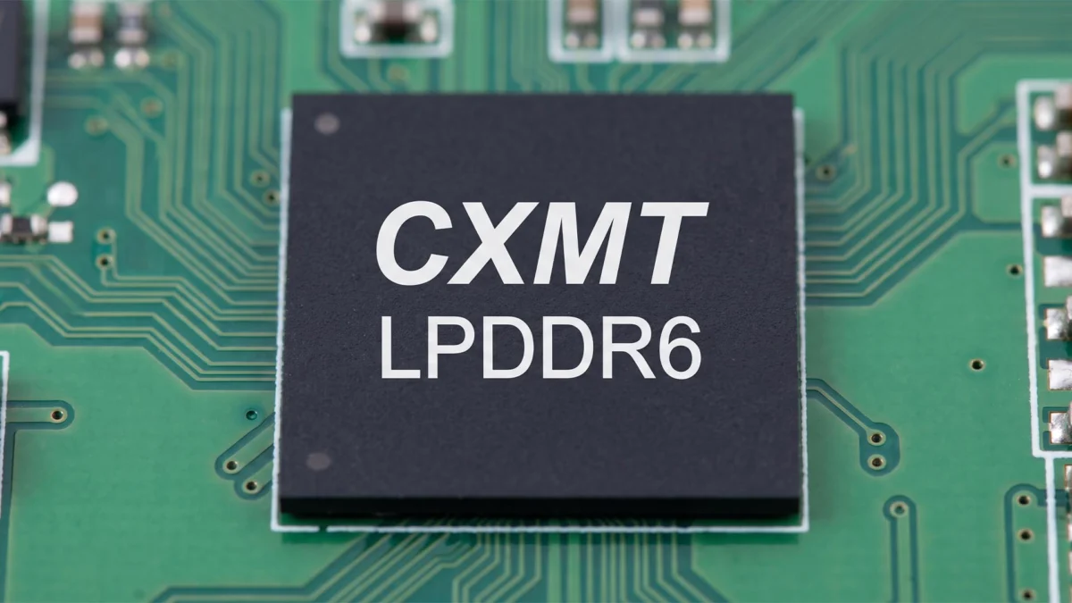
ChangXin Memory Technologies (CXMT), China’s premier manufacturer of dynamic random-access memory (DRAM), is reportedly grappling with severe production inefficiencies as it attempts to break into the high-stakes market for High Bandwidth Memory (HBM). According to recent reports originating from South Korean industry analysts and media outlets, CXMT’s efforts to mass-produce HBM3—the sophisticated memory architecture essential for artificial intelligence (AI) accelerators—have hit a critical bottleneck. The firm’s production yields for 8-layer HBM3 chips are currently estimated to be hovering between 25% and 30%. This figure stands in stark contrast to the yields achieved by global leaders such as SK hynix and Samsung, who have spent years refining the complex stacking and interconnection processes required for HBM.
The struggle highlights the widening chasm between traditional DRAM manufacturing and the advanced packaging requirements of HBM. While CXMT has successfully carved out a significant share of the global legacy memory market by supplying standard DDR4 and LPDDR4 modules, the transition to HBM represents a paradigm shift in complexity. In the legacy market, CXMT benefited from a strategic opening created when top-tier manufacturers like SK hynix, Micron, and Samsung diverted their production lines toward high-margin HBM to satisfy the insatiable demand of the AI data center buildout. However, as CXMT attempts to follow this pivot, it is finding that the "barrier to entry" for HBM is defined less by wafer fabrication and more by the precision of advanced semiconductor packaging.
The Technical Bottleneck: Through Silicon Vias and Stacking Precision
At the heart of CXMT’s production woes is the implementation of Through Silicon Via (TSV) technology. Unlike traditional DRAM, where chips are laid out horizontally on a printed circuit board, HBM involves stacking multiple DRAM dies vertically. To enable communication between these layers and the base logic die, manufacturers must drill thousands of microscopic holes through the silicon wafers and fill them with conductive material, usually copper. These are the TSVs.
According to industry insiders cited by Chosun Biz, a standard CXMT HBM3 chip requires approximately 3,000 TSV cutouts. The precision required to align these vias across eight layers of silicon is infinitesimal. Even a slight misalignment or a microscopic impurity in the conductive fill can lead to a total failure of the memory stack. Reports indicate that CXMT is currently seeing a failure rate where nearly 80 out of every 100 HBM3 chips fail to meet quality clearance during the initial stages of production. Even for the units that do pass initial checks, only about 70% survive the rigorous secondary testing and evaluation required before they can be integrated into end products like AI GPUs.
The complexity is further compounded by the bonding process. To hold the stack together, manufacturers traditionally use "bumps"—microscopic solder balls—between layers. As the industry moves toward HBM3E and the upcoming HBM4, there is a shift toward "hybrid bonding." This method removes the bumps entirely, relying on an underfill material and direct copper-to-copper bonding to reduce the thickness of the stack and improve thermal efficiency. CXMT’s current difficulties with traditional stacking suggest that the leap to hybrid bonding, which requires extreme surface smoothness and ultra-cleanroom environments to prevent contamination, may be even further out of reach for the Hefei-based firm.
Chronology of CXMT’s Expansion and the HBM Pivot
To understand the gravity of these yield issues, one must look at the rapid trajectory of CXMT within the context of China’s broader semiconductor ambitions.

- 2016–2019: CXMT was founded in Hefei with significant state backing. It focused initially on catching up with the DDR4 standard, utilizing a massive influx of capital from the China Integrated Circuit Industry Investment Fund (often called the "Big Fund").
- 2020–2022: The firm successfully stabilized its 19nm and 17nm process nodes, allowing it to become a viable alternative to Western and Korean suppliers for domestic Chinese electronics manufacturers. During this period, US-led export controls began to tighten, emphasizing the need for a domestic HBM solution to power Chinese-made AI chips.
- 2023: As the AI boom triggered by Large Language Models (LLMs) like ChatGPT took hold, global demand for HBM skyrocketed. CXMT announced its intention to enter the HBM market, recognizing that without domestic HBM, China’s AI ambitions (led by firms like Huawei and Biren Technology) would be stunted by international supply chain restrictions.
- Early 2024: Reports surfaced that CXMT had begun ordering specialized equipment for HBM production, including TSV etching tools and bonding machinery.
- Late 2024: The current reports emerge, suggesting that while the hardware is in place, the process maturity is lacking, resulting in the unsustainable 25% yield rate.
Comparative Data: The Yield Gap
In the semiconductor industry, yield is the primary determinant of profitability. For a mature DRAM process, yields typically exceed 90%. For HBM, which is inherently more difficult, the industry gold standard is believed to be between 60% and 80% for established players.
A 25% yield rate means that for every wafer processed, three-quarters of the potential revenue is discarded as scrap. For a company like CXMT, which is already operating under the pressure of heavy capital expenditure and geopolitical scrutiny, such low efficiency creates a massive financial drain. Furthermore, low yields result in inconsistent supply, making it difficult for CXMT to secure long-term contracts with major AI chip designers who require guaranteed volumes of high-performance memory.
The "70% final pass rate" mentioned in the Korean reports adds another layer of concern. This means that even after the expensive and time-consuming process of stacking and bonding is complete, nearly a third of the finished modules are found to be defective during final stress testing. In comparison, the "Big Three"—SK hynix, Samsung, and Micron—have refined their "Known Good Die" (KGD) testing to a point where final assembly failures are minimized, ensuring much higher margins.
Geopolitical Implications and the Quest for Self-Sufficiency
The struggles at CXMT are not merely a corporate hurdle; they are a significant setback for China’s national strategy for semiconductor self-sufficiency. Under the "Made in China 2025" initiative and subsequent policy updates, Beijing has prioritized the domestic production of high-end semiconductors to insulate itself from US Department of Commerce export restrictions.
Currently, the most advanced AI chips, such as NVIDIA’s H100 or Blackwell series, rely exclusively on HBM3 and HBM3E. While the US has restricted the export of these specific GPUs to China, Chinese firms have developed domestic alternatives like the Huawei Ascend 910B. However, these domestic chips still require HBM to function effectively. If CXMT cannot provide a reliable, high-yield supply of HBM, Chinese AI firms will remain dependent on the "gray market" or older, less efficient memory technologies, putting them at a competitive disadvantage in the global AI race.
Furthermore, the equipment necessary to fix these yield problems is often subject to export controls. Advanced TSV etching tools and high-precision bonding machines are produced by a handful of companies, such as Applied Materials, Lam Research, and Tokyo Electron. While CXMT has managed to acquire some of this equipment, the "secret sauce" often lies in the software and process recipes provided by these vendors, which are increasingly difficult to access under current trade regimes.
Market Analysis: The Opportunity Cost
While CXMT struggles with HBM, its absence as a major player in the high-end market has broader implications for the global supply chain. The concentration of HBM production among three companies has led to a supply crunch and soaring prices. Had CXMT entered the market with healthy yields, it could have acted as a price stabilizer and a primary supplier for the "non-AI" sectors that are currently being neglected.

Instead, CXMT’s current situation forces it to remain entrenched in the legacy DRAM market. While this provides steady revenue, it is a low-margin business compared to HBM. There is also the risk of oversupply in the legacy sector; if CXMT and other Chinese firms like JHICC (Fujian Jinhua IC) continue to flood the market with standard DDR4 because they cannot graduate to HBM, it could lead to a price collapse in the very segment that CXMT relies on for survival.
Outlook and Industry Reactions
Industry analysts suggest that CXMT’s path forward will require a fundamental re-evaluation of its packaging strategy. Some suggest that the firm may seek to collaborate with domestic outsourced semiconductor assembly and test (OSAT) giants, such as JCET (Jiangsu Changjiang Electronics Technology), to solve the stacking and bonding issues. By offloading the complex packaging to specialists, CXMT could focus on improving the base DRAM die quality.
However, the internal nature of HBM production—where the die fabrication and stacking are increasingly integrated into a single continuous process—makes outsourcing difficult. Most successful HBM manufacturers have found that tight integration between the wafer fab and the packaging line is essential for high yields.
While CXMT has not issued an official statement regarding the specific yield figures reported in the Korean media, the firm has consistently messaged its commitment to "continuous innovation" and "expanding its product portfolio." Domestic Chinese media have been more optimistic, framing these struggles as the "growing pains" necessary for any firm attempting to master "frontier technologies."
Conclusion
The reports of CXMT’s 25% yield rate serve as a stark reminder that in the semiconductor world, capital and ambition are no substitutes for time and iterative experience. High Bandwidth Memory represents the current pinnacle of memory engineering, and the technical hurdles of TSV implementation and multi-layer stacking remain formidable. As the global AI industry moves toward HBM4 and even more complex 3D-stacked architectures, CXMT faces a race against time. To remain relevant in the next decade of computing, the firm must not only fix its current HBM3 production lines but also bridge a massive technological gap under the most challenging geopolitical conditions in the history of the industry. For now, the "bottleneck" in the global memory industry remains firmly in place, with CXMT struggling to turn the key.