 admin
admin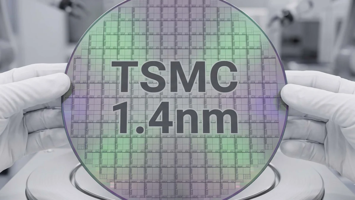
Taiwan Semiconductor Manufacturing Company (TSMC), the world’s preeminent contract chipmaker, is reportedly accelerating its roadmap for the next generation of semiconductor fabrication, with its highly anticipated 1.4-nanometer (1.4nm) process technology now slated for trial production as early as April 2027. Known internally as the "14A" manufacturing node, this technology represents a critical leap in the semiconductor industry’s transition into the "Angstrom Era," succeeding the 2-nanometer (2nm) generation currently under development. According to reports from the Taiwanese press, the development of the 14A node is centered at a massive new facility in the Central Taiwan Science Park in Taichung. The updated schedule indicates that mass production could commence in the second half of 2027, a significant advancement from previous industry projections that placed the 1.4nm rollout in 2028.
Strategic Infrastructure: The Taichung 1.4nm Production Hub
The backbone of TSMC’s 1.4nm ambitions lies in a multi-phase construction project currently underway in Taichung. Reports from the local technology park administration indicate that construction on the first phase of the facility began in October of last year. The site is designed to house four distinct factory units, referred to as P1 through P4, which will collectively form a powerhouse for advanced node manufacturing.
The first factory, P1, has seen rapid progress over the last twelve months. The steel framework of the structure has been fully erected, and construction crews are currently focused on the installation of interior floors and external walls. Based on the current pace of development, the P1 facility is expected to reach structural completion by early 2025. This timeline aligns with the broader goal of beginning equipment move-in and initial testing phases by late 2026.
Simultaneously, work on the second factory, P2, is advancing. Workers have completed the concrete foundation and are currently transitioning to the steel structure phase. If the current construction schedule remains uninterrupted, the P2 facility is projected to be fully built by October 2025. The administration of the Central Taiwan Science Park has noted that TSMC is working in close coordination with local authorities to ensure that utility infrastructure, including high-capacity water and power lines, is scaled to meet the immense demands of 1.4nm fabrication.
Accelerated Timeline: From 2028 to 2027
The most significant takeaway from the recent updates is the compression of the production timeline. Historically, the transition between major nodes (such as from 3nm to 2nm) has followed a two-to-three-year cycle. Original industry roadmaps suggested that while the 2nm node (N2) would enter mass production in late 2025, the 1.4nm (14A) node would likely not reach high-volume manufacturing until 2028.
However, the latest reports suggest that TSMC is aiming for a trial production window in April 2027. Trial production, or "pilot runs," is a crucial stage where the company tests the yield and reliability of the silicon wafers before committing to commercial orders. Moving mass production into the second half of 2027 suggests that TSMC has gained significant confidence in its 14A architecture and the integration of next-generation lithography tools.

As for the latter half of the Taichung expansion, the third and fourth plants (P3 and P4) are currently in the licensing and initial preparation stages. TSMC has already secured the construction license for the P3 facility and is in the final stages of the application process for P2’s secondary permits. These subsequent factories are expected to follow a staggered completion schedule throughout 2028, with approximately six months of separation between each facility’s operational readiness. This phased approach allows TSMC to scale capacity in response to market demand while refining manufacturing techniques learned from the initial P1 and P2 deployments.
The Financial and Technical Scale of the 14A Project
TSMC’s push into 1.4nm is backed by a staggering capital investment of approximately $49 billion. This expenditure covers not only the physical construction of the Taichung fabs but also the acquisition of the world’s most advanced semiconductor manufacturing equipment. Central to the 1.4nm process will be the implementation of High-Numerical Aperture Extreme Ultraviolet (High-NA EUV) lithography machines. These machines, produced exclusively by the Dutch firm ASML, are essential for printing the incredibly fine features required at the 1.4nm level, offering higher resolution and better pattern fidelity than the standard EUV tools used for 5nm and 3nm chips.
Technically, the 14A node will build upon the Gate-All-Around (GAA) transistor architecture, which TSMC is introducing with its 2nm (N2) process. GAA, or nanosheet technology, replaces the traditional FinFET structure that has been the industry standard for over a decade. By surrounding the channel with the gate on all four sides, GAA allows for better control over the electrical current, reducing power leakage and increasing performance. The 1.4nm node is expected to offer a 10% to 15% performance increase over 2nm at the same power level, or a 25% to 30% reduction in power consumption at the same performance level.
Competitive Landscape: The Race for the Angstrom Era
TSMC’s accelerated timeline is a direct response to intensifying competition in the foundry market. Its two primary rivals, Intel and Samsung Electronics, have both announced aggressive roadmaps to reclaim technological leadership.
Intel has been particularly vocal about its "five nodes in four years" strategy, aiming to reach the 1.8nm (Intel 18A) node by 2025. If Intel succeeds, it could potentially leapfrog TSMC in transistor density for the first time in several years. Meanwhile, Samsung was the first to implement GAA technology at the 3nm level and has announced its own plans to begin 1.4nm production by 2027.
By pulling its 1.4nm timeline forward, TSMC aims to maintain its dominant market share, which currently sits at over 60% of the global foundry market. The company’s ability to deliver consistent yields at scale has made it the sole supplier for high-end silicon used by Apple, Nvidia, and AMD. Industry analysts suggest that the acceleration of the 14A node is likely driven by early commitments from these key partners, who are demanding more efficient silicon to power the next generation of Artificial Intelligence (AI) data centers and consumer devices.
Implications for the Global Semiconductor Supply Chain
The development of the Taichung facility is not just a corporate milestone for TSMC but a strategic asset for the global technology ecosystem. As AI applications continue to proliferate, the demand for "compute density"—the ability to pack more processing power into a smaller, more energy-efficient footprint—has reached unprecedented levels. The 1.4nm node is specifically designed to address these requirements, providing the foundation for future AI accelerators, high-performance computing (HPC) platforms, and sophisticated mobile processors.

Furthermore, the concentration of such advanced manufacturing in Taiwan reinforces the island’s role as the "Silicon Shield." The $49 billion investment underscores TSMC’s commitment to its home base, even as it expands its international footprint with new facilities in Arizona, Japan, and Germany. However, the most cutting-edge nodes, such as 14A, are expected to remain exclusive to Taiwan for several years after their introduction to ensure the protection of trade secrets and to capitalize on the existing local supply chain cluster.
Economic Impact and Local Reaction
The expansion in Taichung is expected to have a significant ripple effect on the local economy. Beyond the direct employment of thousands of high-tech engineers and construction workers, the project supports a vast network of equipment suppliers, chemical providers, and logistics firms. The Central Taiwan Science Park has already seen an influx of satellite offices from global vendors such as Applied Materials, Lam Research, and Tokyo Electron, all of whom are essential to the 1.4nm ecosystem.
While TSMC has not issued a formal press release regarding the specific April 2027 trial date, the company’s leadership has frequently stated during quarterly earnings calls that their advanced node development remains "on track" or "ahead of schedule." The submission of applications for temporary offices at the Taichung site is a standard procedural step that signals the transition from heavy structural construction to the refined stages of facility outfitting and personnel deployment.
Conclusion and Future Outlook
The transition to 1.4nm represents one of the most challenging engineering feats in human history. At these dimensions, engineers must contend with quantum tunneling and other physical phenomena that threaten the stability of electronic signals. However, TSMC’s steady progress in Taichung suggests that the company is confident in its ability to overcome these hurdles.
If TSMC successfully executes its trial production in April 2027, it will solidify its position at the apex of the semiconductor industry. The 14A node will likely be the primary engine of growth for the company through the end of the decade, providing the hardware necessary for the next evolution of autonomous systems, generative AI, and advanced telecommunications. As construction continues on the P3 and P4 factories, the world will be watching to see if the "Angstrom Era" arrives ahead of schedule, fundamentally altering the trajectory of global technological development.