 admin
admin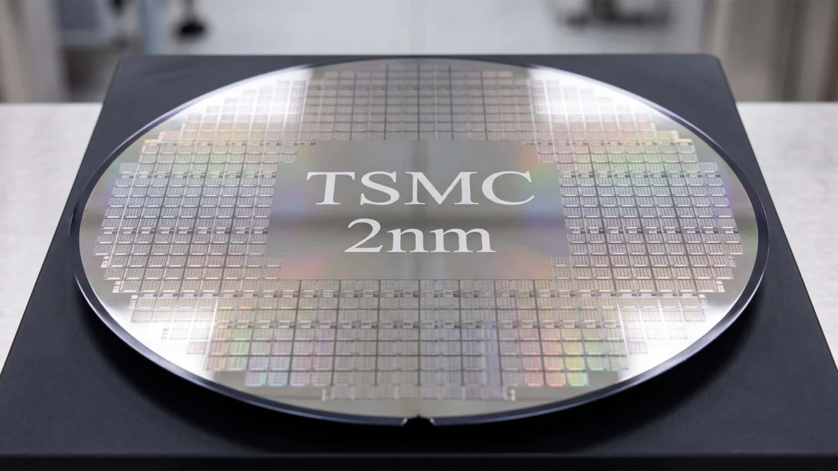
Taiwan Semiconductor Manufacturing Company (TSMC), the world’s preeminent contract chipmaker, has achieved a pivotal operational milestone in its transition toward next-generation lithography. As the company prepares for the commercial debut of its 2nm process technology, internal reports indicate that Fab 20, located in the Hsinchu Science Park, has successfully scaled its production capacity to 20,000 wafers per month. This achievement marks a significant acceleration in TSMC’s roadmap, signaling that the foundry is moving out of the pilot-risk production phase and into a state of readiness for high-volume manufacturing (HVM). The 2nm node, internally designated as N2, represents one of the most significant architectural shifts in the company’s history, transitioning from the long-standing FinFET (Fin Field-Effect Transistor) structure to a sophisticated Gate-All-Around (GAA) nanosheet transistor architecture.
According to data compiled by the Economic Daily News, TSMC has strategically allocated five separate fabrication facilities within Taiwan to focus exclusively on the 2nm ecosystem. While Fab 20 is the current frontrunner in reaching capacity milestones, the collective output of these facilities is expected to underpin the global supply of high-performance computing (HPC) and mobile silicon for the remainder of the decade. Despite the fact that no 2nm products are currently available on the consumer market, the advanced node is already exerting a financial influence on the company’s balance sheet. During recent financial disclosures, it was revealed that 2nm-related activities already contributed approximately 3 percent of the firm’s revenue for the third quarter of 2026, a figure largely driven by research and development partnerships, early-stage tape-outs, and tool installations.
The Technological Evolution: From 3nm FinFET to 2nm Nanosheet
The transition from 3nm (N3) to 2nm (N2) is not merely a shrink in physical dimensions but a fundamental reimagining of how transistors operate. Since the 16nm era, TSMC has utilized FinFET technology, which uses a "fin" shaped channel to control current. However, as dimensions shrunk toward the 3nm threshold, physical limitations—such as current leakage and short-channel effects—began to challenge the efficiency of FinFETs. To overcome these hurdles, the N2 node introduces the Nanosheet transistor. In this design, the gate surrounds the channel on all four sides, providing superior electrostatic control, reducing power consumption, and allowing for higher drive currents.
TSMC’s internal projections suggest that the N2 process will deliver a 10% to 15% speed improvement at the same power levels as the current N3E (3nm enhanced) process. More importantly for the mobile industry, it offers a 25% to 30% reduction in power consumption at the same speed. This efficiency gain is the primary driver behind the aggressive adoption rates seen from smartphone manufacturers like Apple and Google. Furthermore, TSMC is planning a comprehensive N2 family, which will eventually include N2P (featuring backside power delivery) and N2X (optimized for high-performance computing), ensuring a multi-year lifecycle for the 2nm generation.
Chronology of the 2nm Rollout and Fab Expansion
The journey toward 20,000 wafers per month at Fab 20 has been years in the making. TSMC officially announced its 2nm roadmap in 2022, following the successful ramp-up of its 5nm and 4nm nodes. Construction of the Hsinchu and Kaohsiung facilities began shortly thereafter, with the company investing tens of billions of dollars in Extreme Ultraviolet (EUV) lithography equipment and cleanroom infrastructure.
In early 2024, TSMC began installing tools in the first phase of Fab 20. By mid-year, risk production commenced, allowing lead customers to test their designs on actual silicon. The current milestone of 20,000 wafers per month indicates that the yield rates—the percentage of functional chips on a single wafer—have reached a level of stability that justifies increased throughput. Looking ahead, the timeline for the 2nm node follows a strict trajectory:
- Late 2024: Continued scaling of Fab 20 and the beginning of equipment move-in for the Kaohsiung 2nm site.
- Mid-2025: Mass production (HVM) for the first wave of consumer SoCs (System-on-Chips).
- Late 2025: Apple’s anticipated launch of the iPhone 17/18 series featuring N2 silicon.
- 2026: Integration of Backside Power Delivery (BSPD) in the N2P variant to further enhance performance.
Market Demand and Lead Customers: Apple and Google
The appetite for the 2nm node is unprecedented. TSMC management recently confirmed that the N2 process has seen four times as many "tape-outs"—the final stage of the design process before manufacturing begins—compared to the 3nm node at the same point in its lifecycle. This surge is attributed to the dual pressure of the smartphone "performance wars" and the exponential growth of artificial intelligence.
Apple, historically TSMC’s most significant partner, is expected to be the first to market with 2nm technology. Industry analysts predict the A20 Pro chip, slated for the iPhone 18 Pro series, will be the flagship product for the N2 node. By securing the lion’s share of early 2nm capacity, Apple maintains its competitive edge in thermal efficiency and battery life, which are critical as on-device AI features become more resource-intensive.
In a notable shift, Google is also positioning itself as an early adopter. The Pixel 11 series, expected to debut in late 2025 or early 2026, will likely feature the Tensor G6 chip manufactured on TSMC’s 2nm process. This marks a strategic move for Google, which previously relied on Samsung Foundry for its Tensor silicon. Moving to TSMC’s N2 node suggests that Google is prioritizing performance-per-watt to compete more directly with Apple’s hardware-software integration.

The AI Supercycle: NVIDIA, AMD, and the Future of Compute
While smartphones provide the initial volume for new nodes, the long-term revenue driver for TSMC’s 2nm process is undoubtedly the Artificial Intelligence sector. AI accelerators require massive amounts of logic density and extremely low latency, both of which are addressed by the N2 architecture.
Advanced Micro Devices (AMD) has already signaled its intent to utilize the 2nm process for its upcoming MI455X GPU. This "behemoth" chip is designed specifically for Agentic AI—AI systems capable of autonomous reasoning and multi-step task execution. By leveraging N2, AMD aims to pack more transistors into a smaller footprint, allowing for the massive memory bandwidth required by Large Language Models (LLMs).
Similarly, NVIDIA is expected to transition its future "Rubin" architecture to the 2nm node. Following the success of the Hopper and Blackwell architectures, Rubin will represent NVIDIA’s next leap in data center dominance. The shift to 2nm will be essential for NVIDIA to maintain its lead over competitors, as the power constraints of modern data centers make efficiency as valuable as raw throughput.
Comparative Analysis: 2nm vs. 3nm Dominance
Despite the excitement surrounding 2nm, TSMC’s 3nm (N3) node remains the current workhorse of the industry. With a monthly output of approximately 175,000 wafers, the 3nm lithography is still in its "golden age." Major customers like Qualcomm, MediaTek, and Intel are currently saturating 3nm capacity for their latest laptop and mobile processors.
The coexistence of 3nm and 2nm is a deliberate strategy by TSMC. By maintaining high 3nm volumes, the company ensures steady cash flow to fund the astronomical Research and Development (R&D) costs of 2nm and beyond. The "four times more tape-outs" statistic for 2nm suggests that while 3nm is the current volume leader, the industry is skipping or rapidly moving through 3nm iterations to reach the efficiency gains offered by the nanosheet transition of N2.
Financial and Geopolitical Implications
The achievement of the 20,000-wafer milestone at Fab 20 also carries significant weight in the context of global semiconductor competition. TSMC’s primary rivals, Samsung Foundry and Intel Foundry, are also racing to perfect their own 2nm-class nodes (SF2 and Intel 18A, respectively). By demonstrating stable production capacity and high customer engagement, TSMC reinforces its position as the "safe bet" for fabless semiconductor companies.
Financially, the 2nm node is expected to be a major margin driver. While the cost per wafer for 2nm is estimated to be significantly higher than 3nm—due to the complexity of GAA architecture and the requirement for more EUV mask layers—the premium performance it offers allows TSMC to command higher ASPs (Average Selling Prices). Analysts suggest that as yield rates climb, the 2nm node will eventually eclipse 3nm in total revenue contribution by 2027.
Furthermore, the concentration of 2nm production in Taiwan highlights the island’s continued importance in the global technology supply chain. Despite TSMC’s expansion into Arizona, Germany, and Japan, the most advanced "bleeding-edge" nodes remain anchored in domestic fabs like Fab 20. This "Silicon Shield" continues to be a focal point of international trade discussions and regional security.
Conclusion and Outlook
TSMC’s successful ramp-up to 20,000 monthly wafers at its 2nm facility is more than just a production stat; it is a signal to the tech industry that the next era of computing is ready for deployment. As Apple and Google prepare to bring the first 2nm-powered devices to consumers, and as AI giants like NVIDIA and AMD prepare their next-generation data center architectures, the semiconductor landscape is poised for a dramatic shift in power and efficiency.
With five fabs dedicated to this new lithography and a robust pipeline of designs ready for manufacturing, TSMC appears to have successfully navigated the most difficult transition in transistor design in over a decade. The industry now looks toward 2025, when the first 2nm chips will officially enter the hands of consumers, setting a new benchmark for what is possible in silicon engineering.