 admin
admin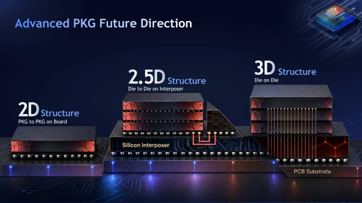
At the Hot Chips 2026 symposium, a premier forum for high-performance microprocessors and integrated circuits, SK Hynix Vice President of Package Engineering Jaesik Lee detailed the company’s strategic roadmap for High-Bandwidth Memory (HBM). The presentation, titled "Advanced Packaging for High-Bandwidth Memory," outlined a comprehensive shift in semiconductor architecture as the industry transitions from 2.5D configurations to fully realized 3D packaging. As the demand for artificial intelligence (AI) and high-performance computing (HPC) continues to outpace traditional memory scaling, SK Hynix is positioning advanced packaging not merely as a protective housing, but as a critical performance enabler.

The core of the presentation focused on the evolution of HBM4 and the specialized packaging techniques required to sustain the relentless demand for bandwidth. By integrating technologies such as Intel’s Embedded Multi-die Interconnect Bridge (EMIB) and moving toward hybrid bonding, SK Hynix aims to overcome the physical limitations of current silicon interposers. This transition marks a pivotal moment in the memory industry, where the boundaries between memory and logic are increasingly blurred to satisfy the data-hungry requirements of next-generation large language models and autonomous systems.

The Architecture of Modern HBM and the Scaling Imperative
To understand the trajectory toward HBM4 and beyond, the current state of HBM3E provides the necessary baseline. High-Bandwidth Memory is characterized by its 3D stacked structure, which connects multiple core dies—DRAM integrated circuits (ICs)—to a base die using Through-Silicon Vias (TSVs). Current high-end solutions utilize a 16-Hi stack, reaching a maximum height of 16 slices. This structure is organized into four ranks, with each slice incorporating four channels and 16 banks.

The primary advantage of HBM over traditional memory solutions like GDDR6 lies in its efficiency across three vectors: space, power, and bandwidth. For instance, a standard GDDR6 configuration typically offers 24 GB of capacity and 768 GB/s of bandwidth. In contrast, an HBM3E solution with just four stacks can provide up to 144 GB of capacity and 4 TB/s of bandwidth while occupying approximately half the physical footprint on a printed circuit board (PCB). This density is achieved by mounting the HBM and the processor (GPU or XPU) on the same silicon interposer using 2.5D packaging. Each HBM module utilizes 1024 I/Os across 16 channels, connecting to the processor’s physical layer (PHY) through the interposer.

As the industry moves toward HBM4, these specifications are set to expand significantly. SK Hynix’s roadmap identifies HBM4 as the upcoming flagship, utilizing 24 Gb DRAM densities to achieve stack capacities of 36 GB. The interface will double from 1024 to 2048 I/O bits, with I/O speeds reaching 8 Gbps. This results in a total bandwidth of 2048 GB/s per stack, a milestone necessary to support the projected computational requirements of 2027 and 2028.

Packaging Methodologies: The Battle Between TC-NCF and MR-MUF
A critical portion of Jaesik Lee’s presentation addressed the competing manufacturing processes used to assemble these complex stacks. Currently, the industry is divided between two primary technologies: Thermo-Compression with Non-Conductive Film (TC-NCF) and Mass Reflow with Molded Underfill (MR-MUF).

TC-NCF is a method favored by some competitors for its ability to mitigate die warpage, a common issue when stacking extremely thin layers of silicon. However, TC-NCF suffers from higher thermal resistivity and lower overall productivity due to the precision required for each individual layer. SK Hynix, conversely, has championed the MR-MUF process. By utilizing a liquid underfill material that is injected and then hardened, MR-MUF offers superior productivity and significantly lower thermal resistivity. While historically more susceptible to chip warpage, SK Hynix has introduced "Advanced MR-MUF" to resolve these drawbacks.

For the 16-Hi HBM3E solution, SK Hynix implemented Warpage Control and Fine Pitch Interconnection technologies. This allowed the company to increase the total package height to 775 microns while simultaneously shrinking the chip thickness to 0.9x and reducing the bump pitch. These refinements ensure that as the stacks get taller, they remain structurally sound and thermally efficient.

Addressing the Thermal Burden and Power Delivery Challenges
The transition to HBM4 brings formidable challenges, most notably the "Thermal Burden." SK Hynix data suggests that as bandwidth doubles every two generations, the thermal load on the packaging increases by a factor of 2.2x. This is compounded by the "Area Penalty" of TSVs. Even as the pitch size of these vias shrinks, the sheer number of connections required for HBM4—which will exceed 20,000 TSVs per stack—takes up an increasing percentage of the silicon real estate.

To mitigate these hotspots, SK Hynix is developing I-HBM (Integrated HBM) technology. Similar to Samsung’s Heat Path Block (HPB), I-HBM involves embedding a high-thermal-conductivity, electrically insulating cooling component directly into the HBM device-to-device (D2D) PHY area. This is the region where localized hotspots are most prevalent. By creating a dedicated heat path, SK Hynix claims a reduction in thermal resistance of more than 30%.

Power delivery is another bottleneck. As HBM power consumption trends upward to meet bandwidth demands, it risks exceeding the limits of existing system power delivery networks (PDN). SK Hynix plans to address this by leveraging advanced logic foundry processes for the base die. By spreading power TSVs "everywhere" throughout the stack, the company expects to improve PDN efficiency by up to 75%, ensuring stable voltage even during peak computational loads.

The Shift to Hybrid Bonding and 3D Integration
As the industry looks beyond 16-Hi stacks toward 20-Hi or 24-Hi configurations, traditional solder-based micro-bumps reach their physical limit. SK Hynix is therefore aggressively pursuing Hybrid Bonding (Cu-to-Cu) for the HBM4E era.

Hybrid bonding eliminates the need for traditional bumps by directly fusing the copper pads of one die to another. This results in several advantages:

- Reduced Pitch: TSV pitch can be reduced to below 18 microns.
- Increased Die Thickness: Because the bonding layer is so thin, the individual DRAM core dies can be 24% thicker, which improves structural integrity and manufacturing yield.
- Thermal Efficiency: Hybrid bonding offers 35% lower thermal resistance compared to MR-MUF, as the direct copper-to-copper connection acts as a highly efficient heat conductor.
The ultimate goal of this roadmap is true 3D integration. In this scenario, HBM stacks would no longer sit beside the processor on an interposer but would be stacked directly on top of the logic accelerator. This "HBM-on-Logic" approach would virtually eliminate the latency associated with the silicon interposer and drastically reduce the energy required to move data between memory and the compute engine.

Strategic Partnerships and Industry Implications
The presentation also shed light on the collaborative nature of the semiconductor ecosystem. SK Hynix highlighted its compatibility with various 2.5D packaging standards, including TSMC’s CoWoS (Chip on Wafer on Substrate) variants (CoWoS-S, CoWoS-L, and CoWoS-R) and Intel’s EMIB technology.

The inclusion of Intel’s EMIB in the roadmap is particularly noteworthy. EMIB uses a small silicon "bridge" embedded in the substrate to connect dies, offering a more cost-effective alternative to large silicon interposers while maintaining high-speed connectivity. This alignment adds weight to ongoing rumors regarding a joint venture between Intel and SK Hynix. Reports have suggested a potential $28 billion collaboration, possibly involving Intel’s upcoming fabrication facilities in Ohio, to secure a domestic U.S. supply chain for high-end AI memory.

The broader implications for the technology sector are significant. As AI models grow in complexity, the "memory wall"—the gap between processor speed and memory access speed—becomes the primary bottleneck for innovation. SK Hynix’s aggressive pursuit of HBM4 and 3D packaging suggests that the industry is moving toward a more holistic design philosophy. In this new era, memory is no longer a commodity component but a custom-engineered logic-memory hybrid tailored for specific AI workloads.

Conclusion: The Path to 2028 and Beyond
The roadmap presented at Hot Chips 2026 underscores a relentless drive toward higher power density and bandwidth. Success in the HBM4 era will require more than just narrower pitches and taller stacks; it will demand a total co-optimization of materials science, thermal engineering, and cross-industry collaboration.

With innovations like Advanced MR-MUF, I-HBM cooling, and the impending transition to hybrid bonding, SK Hynix is attempting to stay ahead of a curve that is steepening. As the company moves toward 2028, the focus will remain on refining the 3D integration of HBM with logic, a move that promises to redefine the performance limits of the global AI infrastructure. The integration of Intel’s EMIB and the potential for new foundry partnerships indicate that the next decade of semiconductor dominance will be won by those who can best manage the complex physics of advanced packaging.