 admin
admin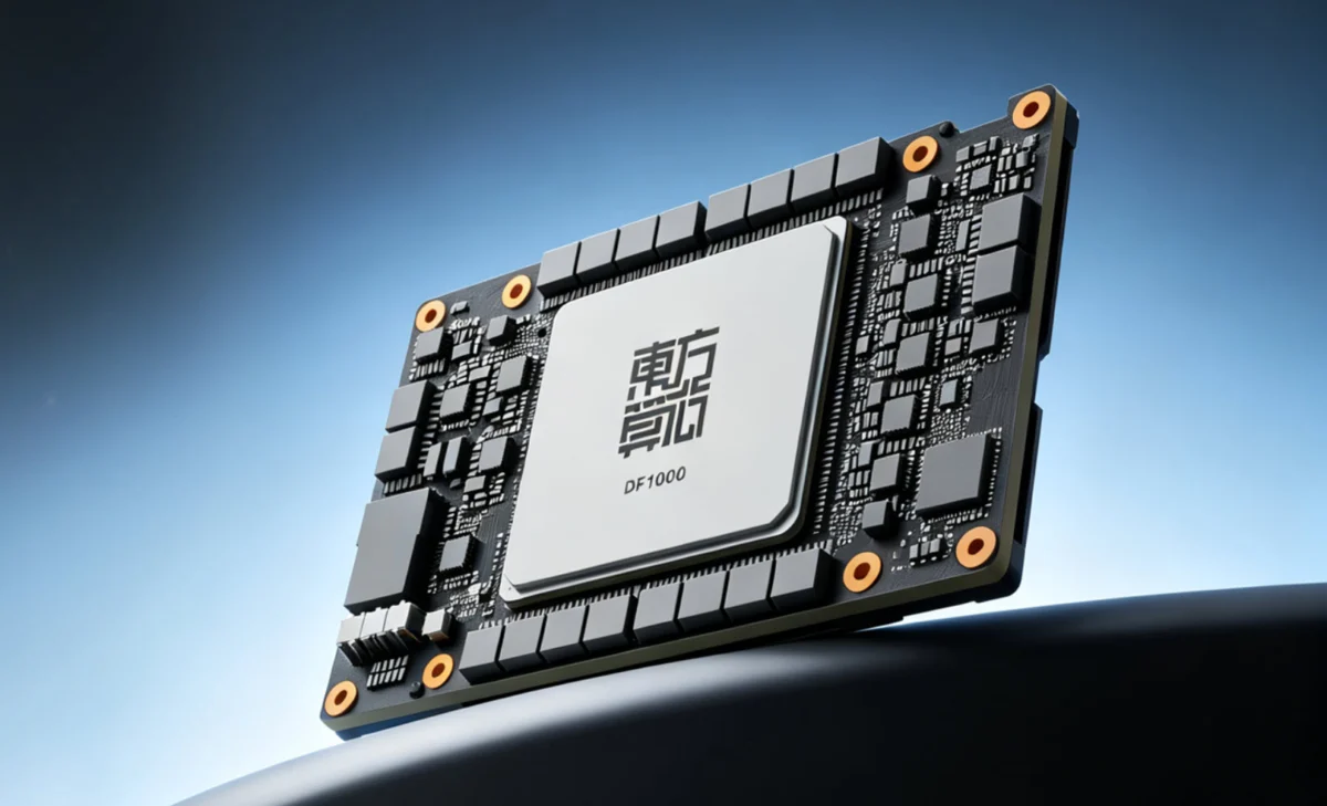
The global semiconductor landscape is currently witnessing a strategic shift as China’s Dongfang Suanxin (DFSX) attempts to redefine the benchmarks of artificial intelligence (AI) hardware performance. By prioritizing memory bandwidth over the industry’s long-standing obsession with process node miniaturization, DFSX is positioning its upcoming DF2000 chips and TY64 SuperNode systems as direct competitors to NVIDIA’s market-leading Blackwell-based GB200 NVL72. This architectural pivot suggests that the future of AI scaling may not lie in the pursuit of sub-5nm transistors, but rather in overcoming the "memory wall"—the bottleneck where high-performance GPUs remain idle while waiting for data to be retrieved from memory layers.
The Architectural Shift: Memory Bandwidth vs. Node Miniaturization
For decades, Moore’s Law has dictated that the primary path to increased computational power is the shrinking of transistors. However, as the industry approaches the physical limits of silicon, the gains from moving to 3nm or 2nm nodes have become increasingly marginal compared to the soaring costs of development and fabrication. DFSX is operating on a different hypothesis: that for large language models (LLMs) and massive AI workloads, the efficiency of data movement is more critical than raw floating-point operations per second (FLOPS).
The company’s DF1000 and the subsequent DF2000 chips are fabricated using a mature 14nm process. While 14nm is several generations behind the 4nm and 3nm nodes used by NVIDIA and TSMC, DFSX compensates for this by utilizing a sophisticated 3D near-memory compute architecture. In a traditional chip design, memory and logic are separate components connected by horizontal pathways. In the DFSX model, memory is stacked directly on top of the compute layer. This connection is achieved through 3D wafer-level hybrid bonding, a process that melds the copper pathways of the two layers directly. By eliminating the need for traditional microbumps or wires, the architecture creates tens of millions of vertical interconnects, functioning as high-speed elevators rather than a congested horizontal highway.
Evolution of the DFSX Product Line: From DF1000 to DF2000
The DF1000 served as the proof-of-concept for this vertical integration, demonstrating that mature nodes could achieve competitive throughput when the distance between memory and logic was minimized. The upcoming DF2000, slated for a Q4 2026 debut, scales this concept significantly. The DF2000 introduces what the company calls a "3.5D Infinity Chiplet" layout. This design does not merely stack a single memory layer; instead, it combines multiple stacked memory-compute towers on a unified base foundation.
Central to the DF2000’s performance is its custom-engineered 3D Dynamic Random-Access Memory (DRAM). By replacing standard storage layers with this proprietary 3D DRAM, DFSX has dramatically increased the volume of temporary data that can be held directly within the chip structure. This allows the processor to handle much larger datasets without needing to fetch information from external memory modules, which is the primary cause of latency in modern AI training and inference.
Comparative Analysis: TY64 SuperNode vs. NVIDIA GB200 NVL72
The true scale of DFSX’s ambition is revealed when these chips are arrayed into the TY64 SuperNode. A single DF2000 chip is engineered to offer a memory bandwidth of 15TB/s. When 64 of these chips are integrated into a TY64 SuperNode, the aggregate memory bandwidth reaches a staggering 960TB/s.
To put this in perspective, NVIDIA’s flagship GB200 NVL72 system, which utilizes the highly advanced Blackwell architecture on a 4nm-class process, offers a total memory bandwidth of approximately 576TB/s. The DFSX system, despite being built on "inferior" 14nm lithography, provides nearly 67% more bandwidth than NVIDIA’s current top-tier offering.
However, the trade-offs of using a mature node remain evident in raw compute power. The DF2000-based TY64 SuperNode is rated at 64 PFLOPS of BF16 compute. In contrast, the NVIDIA GB200 NVL72 delivers roughly 360 PFLOPS of BF16 compute. This six-fold difference in raw floating-point performance highlights the gap in transistor density. Nevertheless, DFSX argues that in real-world AI applications—particularly inference for massive models—the 960TB/s bandwidth ensures that the 64 PFLOPS are utilized at near-maximum efficiency, whereas the NVIDIA system may face diminishing returns as its faster cores wait for data to catch up.

The Problem of the "Memory Wall" in AI Workloads
The "memory wall" is a well-documented phenomenon in computer architecture where the improvement in processor speed far outpaces the improvement in memory access time. In the context of AI, this means that even the fastest GPUs spend a significant portion of their operational cycles "starved" of data. As LLMs grow in parameters, the amount of data that must be moved in and out of the processor increases exponentially.
DFSX’s strategy is built on the belief that FLOPS is the wrong metric for the current era of AI. As flagship models continue to expand, the primary throughput-limiting factor has shifted from per-chip compute to system-level integration, interconnect speed, and memory bandwidth. By focusing on the 3D hybrid bonding and 3.5D chiplet architecture, DFSX aims to bypass the limitations of 14nm lithography by ensuring that every bit of compute power available is constantly fed with data.
Chronology and Future Roadmap: The Path to DF3000
The development timeline for DFSX indicates a rapid iteration cycle designed to close the gap with global leaders.
- 2024-2025: Deployment and testing of the DF1000, establishing the viability of 3D near-memory compute on 14nm nodes.
- Q4 2026: Expected launch of the DF2000 chip and the TY64 SuperNode, targeting 15TB/s per chip and 960TB/s per node.
- Post-2026: Development of the DF3000 series. Early projections suggest the DF3000 will offer 20TB/s of memory bandwidth per chip. When arrayed in a TY64 SuperNode configuration, this would result in a total bandwidth of 1,280TB/s.
For comparison, NVIDIA’s future "Vera Rubin" NVL72 system is expected to offer a total memory bandwidth of approximately 1,580TB/s. While the NVIDIA system will still hold the lead, the gap is narrowing. The DF3000-based system would be only 23% behind the Rubin-based system in bandwidth, a remarkable feat considering the likely disparity in the underlying process nodes.
Geopolitical and Economic Implications
The emergence of DFSX is also a reflection of the current geopolitical climate. Faced with stringent export controls that limit access to the most advanced Extreme Ultraviolet (EUV) lithography machines, Chinese semiconductor firms have been forced to innovate within the constraints of mature nodes like 14nm and 28nm.
By mastering advanced packaging techniques like 3D hybrid bonding, DFSX is demonstrating a "pathway around" the sanctions. If a 14nm chip with superior packaging can perform specialized AI tasks as effectively as a 4nm chip with traditional packaging, the economic and strategic value of the most advanced nodes may be re-evaluated. Furthermore, the use of 14nm nodes allows for higher yields and lower production costs compared to the cutting-edge nodes, potentially offering a better price-to-performance ratio for enterprise-level AI deployments.
Industry Reactions and Market Outlook
Industry analysts have expressed a mix of skepticism and intrigue regarding DFSX’s claims. On one hand, the disparity in BF16 compute power (64 PFLOPS vs. 360 PFLOPS) is a significant hurdle for training the largest foundation models, where raw horsepower is essential. Critics argue that while bandwidth is vital for inference, training still requires the massive parallel processing power that only high-density nodes can provide.
On the other hand, the shift toward "edge AI" and specialized enterprise LLMs makes inference speed a primary concern for many businesses. If the TY64 SuperNode can deliver faster inference times for large models due to its superior bandwidth, it could find a substantial market among cloud service providers and research institutions.
As the industry moves toward 2026, the competition between NVIDIA’s architectural refinements and DFSX’s memory-centric innovations will likely define the next phase of the AI hardware race. The success of the DF2000 will serve as a critical test case for whether advanced packaging can truly compensate for trailing-edge lithography in the most demanding computational environments. For now, Dongfang Suanxin remains a pivotal player to watch, representing a distinct, bandwidth-first philosophy in an industry that has long been obsessed with the size of the transistor.