Tesla Chief Executive Officer Elon Musk has formally introduced TeraFab, a massive semiconductor manufacturing initiative designed to address what he describes as a critical global shortage of high-end computing capacity. During a comprehensive technical showcase, Musk outlined a strategy that positions Tesla not merely as an automotive or energy company, but as a primary architect of the hardware infrastructure required for the next century of civilization. The project, which is slated for development in Austin, Texas, aims to achieve a production scale that Musk claims will eventually dwarf the combined output of current industry leaders such as TSMC, Samsung, and Intel.
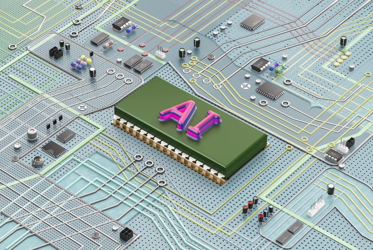
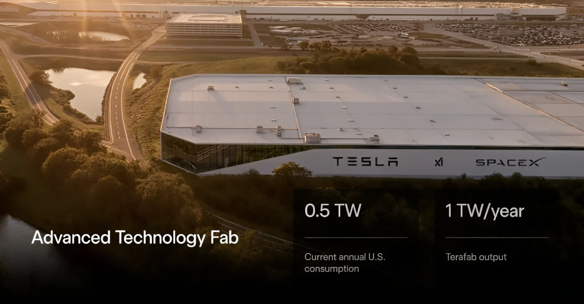
The core premise of TeraFab rests on the assertion that the current global supply of semiconductors meets only a small fraction of the anticipated demand for artificial intelligence (AI) and autonomous systems. According to Musk, the world’s existing fab infrastructure provides only 2% of the compute power that his companies—including Tesla, SpaceX, and xAI—will require to achieve their long-term goals of planetary autonomy and multi-planetary expansion. TeraFab is intended to bridge this 98% gap by producing one terawatt of compute power annually, encompassing the entire lifecycle of chip production from design and masking to fabrication and advanced packaging.
The Architecture of Recursive Improvement
At the heart of TeraFab is a manufacturing philosophy Musk refers to as "rapid, recursive improvement." Unlike traditional semiconductor foundries that operate as third-party contractors for various fabless designers, TeraFab is designed to be a closed-loop, vertically integrated ecosystem. Musk noted that the facility would house every stage of the semiconductor supply chain under one roof. This includes the creation of lithography masks, the fabrication of logic and memory chips, rigorous testing protocols, and advanced 2.5D and 3D packaging.
By unifying these traditionally disparate processes, Tesla intends to create a feedback loop that allows for the immediate refinement of chip designs. Musk explained that if a test reveals a potential optimization in a chip’s architecture, the facility can produce a new mask and a revised prototype within days rather than the months-long cycles typical of current industry standards. This "recursive loop" is intended to accelerate the development of Tesla’s proprietary silicon, moving from the current AI5 architecture to future generations with unprecedented speed.
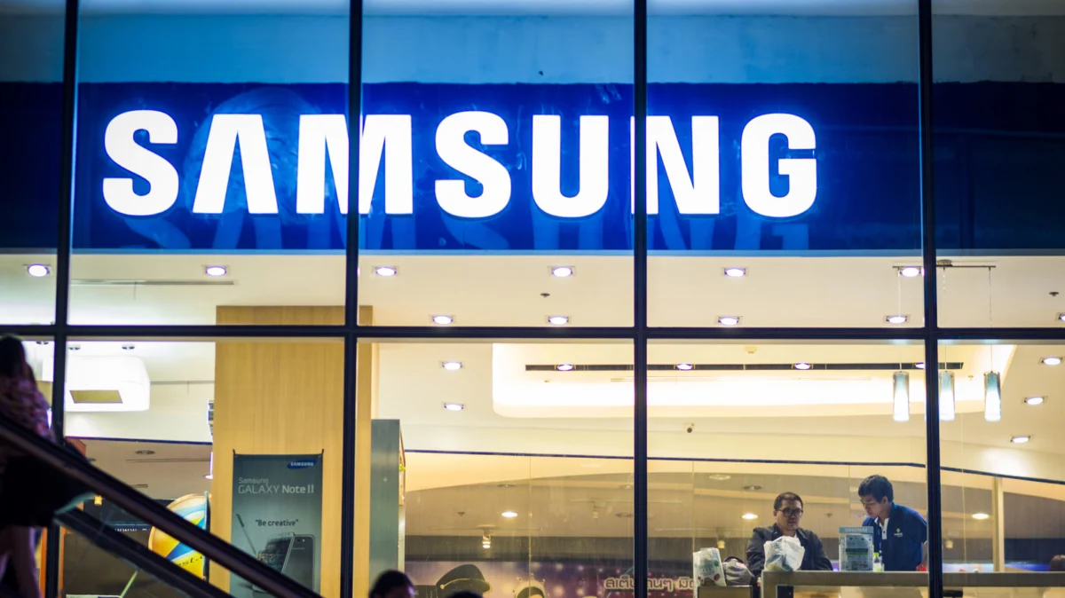
The facility is expected to focus on the 2nm process node from its inception. While the semiconductor industry has historically moved incrementally through process nodes, Tesla’s decision to jump directly to 2nm reflects a "bleeding-edge" approach. Reports suggest that Tesla may explore licensing agreements with Samsung to facilitate the initial 2nm production ramp-up, though the long-term goal remains total self-sufficiency.
Historical Context: From FSD Hardware to TeraFab
The announcement of TeraFab is the culmination of a decade-long transition for Tesla. The company’s foray into custom silicon began in earnest with the development of the Full Self-Driving (FSD) Computer (Hardware 3), which replaced NVIDIA hardware in 2019. This was followed by the introduction of the Dojo supercomputer and its D1 chip, designed specifically for AI training.

Musk’s decision to move into high-volume manufacturing is driven by the scaling requirements of Tesla’s three primary AI pillars: the FSD software suite, the Robotaxi platform, and the Optimus humanoid robot. Each of these products requires massive amounts of inference and training compute. The AI5 chip, which Musk identified as TeraFab’s first major product, is expected to offer significant performance-per-watt improvements over the current Hardware 4, providing the necessary "intelligence" for Optimus to navigate complex human environments.
The Space-Based Compute Strategy
Perhaps the most unconventional aspect of the TeraFab project is the intended deployment of its output. Musk revealed that 80% of the compute power generated by TeraFab will be destined for space. This decision is rooted in the physical and environmental constraints of Earth-based data centers. High-performance AI clusters require immense amounts of electricity and cooling, which Musk argues will eventually become a limiting factor for terrestrial growth.
To circumvent these constraints, Tesla plans to utilize SpaceX’s Starship launch system to deploy "terawatts" of compute power into orbit. These space-based data centers will utilize the D3 chip, a newly unveiled unit specifically engineered for the harsh radiation and thermal environments of space. By leveraging direct solar energy and the vacuum of space for thermal management (through advanced radiative cooling), Musk envisions a galactic computing network that bypasses Earth’s power grid limitations.
The remaining 20% of TeraFab’s output will be dedicated to ground-based applications, primarily the AI5 chips that will power the growing fleet of Tesla vehicles and robots. This bifurcated strategy ensures that while the immediate needs of Tesla’s consumer products are met, the groundwork is laid for a "galactic civilization" powered by orbital AI.
Comparative Scale and Industry Impact
The scale of TeraFab has invited immediate comparison to the "Big Three" of the semiconductor world: TSMC, Intel, and Samsung. Musk’s claim that TeraFab will produce 50 times the compute power of all existing fabs combined is a staggering assertion that has met with both intrigue and skepticism from industry analysts.
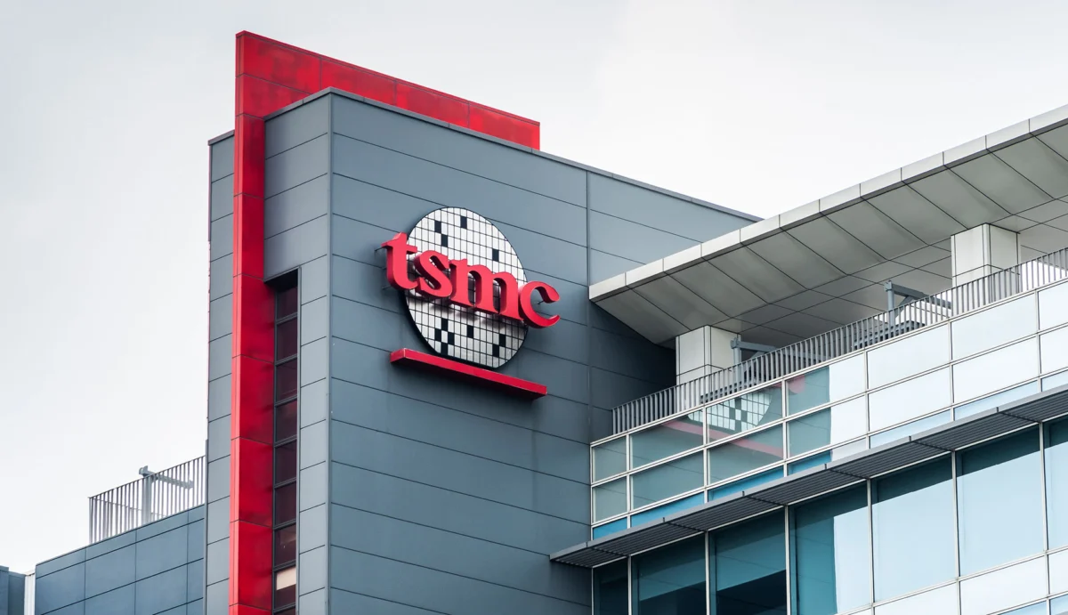
Currently, the semiconductor industry is defined by high specialization. TSMC dominates the foundry market with a focus on cutting-edge logic, while companies like Micron and SK Hynix lead in memory. TeraFab’s goal of integrating logic, memory, and packaging at such a massive scale challenges the fundamental structure of the global supply chain. Musk acknowledged the contributions of current partners like TSMC and Samsung, stating he is "very grateful" for their support. However, he emphasized that their expansion rates are insufficient for Tesla’s "impossible" timelines.
Industry experts point to several significant hurdles that Tesla must overcome to realize this vision:

- Lithography Equipment: The global supply of High-NA EUV (Extreme Ultraviolet) lithography machines is currently controlled by ASML. Securing the dozens of machines required for a "terawatt-scale" facility would require Tesla to navigate a years-long backlog.
- Cleanroom Standards: Semiconductor manufacturing typically requires ultra-clean environments (Class 1 or better). Musk has previously dismissed the necessity of traditional cleanrooms, suggesting that the "machine that builds the machine" can be designed to maintain purity at the wafer level rather than the room level.
- Yield Rates: Achieving high yields on a 2nm process is notoriously difficult. Even established players like Intel have faced multi-year delays when transitioning to new nodes.
Economic and Geopolitical Implications
The decision to build TeraFab in Austin, Texas, carries significant geopolitical weight. As the United States seeks to "re-shore" semiconductor manufacturing through the CHIPS and Science Act, Tesla’s massive private investment aligns with national interests of reducing reliance on overseas foundries. However, TeraFab’s unique focus on internal consumption and space deployment sets it apart from the commercial foundries currently being subsidized by the government.
From a market perspective, TeraFab represents a potential "black swan" event for the AI hardware sector. If Tesla successfully produces its own high-performance silicon at scale, its reliance on NVIDIA for AI training will vanish, potentially shifting billions of dollars in capital expenditure in-house. This vertical integration could provide Tesla with a permanent cost advantage in the robotics and autonomous vehicle markets.
Timeline and Future Outlook
While a specific date for the first "wafer out" at TeraFab has not been confirmed, Musk’s history with "Gigafactories" suggests an aggressive construction schedule. The project is expected to be a joint effort, drawing engineering talent from Tesla’s automotive division, SpaceX’s materials science teams, and xAI’s software architects.
The D3 and AI5 chips represent the first generation of TeraFab’s output, but the long-term roadmap includes even more advanced iterations. Musk’s vision of a "recursive" facility implies that the TeraFab of 2030 will look fundamentally different from the one that breaks ground today, as the AI systems it produces will eventually be used to optimize the manufacturing process itself.
In conclusion, TeraFab is more than a factory; it is a manifestation of Musk’s belief that compute power is the most valuable commodity of the 21st century. By attempting to consolidate the entire semiconductor stack and expanding into orbit, Tesla is attempting to decouple its growth from the limitations of the traditional global economy. Whether TeraFab can meet its ambitious "terawatt" goal remains to be seen, but the project has already succeeded in redefining the scale of what is considered possible in the semiconductor industry. As construction begins in Austin, the tech world will be watching closely to see if Musk can once again disrupt a century-old industry through sheer force of vertical integration.