 admin
admin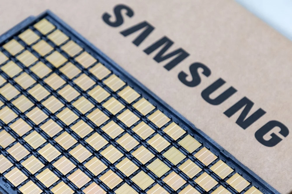
The cornerstone of Samsung’s strategy is the radical transformation of the HBM base die (B-die). Historically, the base die has served as a relatively passive interface, facilitating communication between the stacked DRAM layers (C-die) and the host processor (XPU). However, as AI models grow in complexity and context windows expand into the millions of tokens, the traditional HBM architecture faces severe limitations in bandwidth scaling, power efficiency, and thermal management. Samsung’s response is a three-phase transition that leverages advanced logic manufacturing processes, such as 4nm technology, to turn the base die into a functional extension of the processor itself.

The Architectural Foundation of Modern HBM
To understand Samsung’s roadmap, it is essential to review the current state of HBM architecture. Standard HBM consists of a vertical stack of Core Dies (C-dies) connected via Through-Silicon Vias (TSVs). At the bottom of this stack lies the Base Die (B-die), which contains the physical layer (PHY) and test circuitry. This entire assembly is typically placed alongside a Graphics Processing Unit (GPU) or Tensor Processing Unit (TPU) on a 2.5D silicon interposer.

While this approach has served the industry through the generations of HBM2 and HBM3, the move toward HBM4 and beyond introduces significant bottlenecks. Current scaling efforts are hindered by the density of TSVs, the pitch limits of micro-bumps, and the power consumption of the PHY I/O. Samsung’s data indicates that as bandwidth requirements exceed 3 TB/s per stack in the HBM4 generation and target over 6 TB/s for HBM5, the industry can no longer rely on simple iterative improvements. The gap between the logic processes used for the XPU (often 5nm or 3nm) and the B-die (traditionally older, less efficient nodes) must be closed to enable higher performance.

Phase One: Logic Integration and Area Reclamation
The first phase of Samsung’s roadmap focuses on "XPU Area Reclamation." By migrating the HBM base die to an advanced 4nm logic process, Samsung aims to offload critical functions from the expensive and space-constrained AI processor (the XPU) onto the HBM stack itself. One of the primary candidates for this migration is the memory controller.

Traditionally, the memory controller resides on the XPU, occupying valuable silicon real estate that could otherwise be used for additional compute cores or larger caches. By moving the memory controller to the 4nm B-die, Samsung estimates that 5% to 10% of the XPU area can be reclaimed. This area reduction translates directly into a 10% to 20% performance boost for the processor by allowing for increased compute density.

Furthermore, Phase One introduces the Heat Path Block (HPB) technology. One of the greatest challenges of stacking memory is the accumulation of heat, particularly at the PHY where high-speed data transfer occurs. Samsung’s HPB solution is designed to cover 50% of the PHY area, reducing peak temperatures by over 35%. This thermal headroom is critical for maintaining the reliability of HBM4 and HBM4E stacks, which are expected to reach up to 16-Hi (16 layers) configurations.

Phase Two: Functional Expansion and the Intelligent Base Die
The second phase moves beyond simple area reclamation to "Functional Expansion." In this stage, the base die becomes an active participant in the AI system’s logic. Samsung proposes the integration of advanced Reliability, Availability, and Serviceability (RAS) sensors and real-time telemetry within the B-die. This allows the system to monitor the health of the DRAM cells and the interconnects in real-time, facilitating proactive maintenance and improved yields during manufacturing.

A significant innovation in Phase Two is the introduction of a Near-Memory Controller (Near-MC) "SRAM-Base" cell repair scheme. As DRAM manufacturing reaches the limits of physics, cell-level failures become more common. Samsung’s plan involves using unused space on the logic-based B-die to house SRAM resources. These resources act as a "spare tire," allowing the memory controller to redirect data from a failing DRAM cell to a functional SRAM cell in the base die seamlessly.

Additionally, Samsung is exploring the concept of "AHBM" or Advanced HBM, which incorporates selective processing elements (PEs) directly into the base die. This is a form of Processing-in-Memory (PIM) that allows the memory stack to perform simple computational tasks, such as data filtering or basic arithmetic, before passing the data to the XPU. This reduces the amount of data that must travel across the power-hungry Die-to-Die (D2D) interface, significantly lowering the total system power consumption.

Phase Three: The Transition to 3D ZHBM Convergence
The final and most ambitious phase of the roadmap is the realization of True 3D ZHBM. This represents a paradigm shift from 2.5D packaging to full 3D vertical integration. In the ZHBM (Zero-height or 3D HBM) model, the DRAM stack is no longer placed alongside the XPU on an interposer; instead, it is stacked directly on top of the compute die.

This vertical integration eliminates the need for a 2.5D interposer, which is currently a major cost driver and a source of manufacturing complexity for AI systems like NVIDIA’s H100 or Blackwell series. By utilizing Wafer-on-Wafer (WoW) bonding and Hybrid Cube Bonding (HCB), Samsung can achieve ultra-high I/O density. The data travel distance is reduced from millimeters to micrometers, leading to a projected I/O power efficiency of approximately 0.5 pJ/bit.

The performance metrics for ZHBM are staggering. Compared to standard HBM4E solutions, Samsung projects that ZHBM will offer a 230% increase in DRAM bandwidth and a 70% reduction in DRAM power consumption. Perhaps most importantly for the next generation of AI hardware, the 3D structure is expected to save up to 100W of power per DRAM module. This saved power can be redirected to the GPU cores, providing roughly 8.3% more power for pure computation within the same thermal design power (TDP) envelope.

Chronology of Development and Industry Implications
Samsung’s timeline for these innovations aligns with the projected release cycles of major AI hardware. The transition to HBM4 is expected to begin in the 2025–2026 timeframe, marking the start of Phase One. HBM5 and the initial forays into custom B-die logic (Phase Two) are slated for 2027 and beyond. The full realization of 3D ZHBM (Phase Three) represents the long-term goal for the late 2020s.

The implications of this roadmap for the semiconductor industry are profound. For years, the industry has operated under a "disaggregated" model where memory and logic were treated as separate commodities. Samsung’s move toward custom HBM and 3D integration signals the end of the "one-size-fits-all" memory era. Cloud service providers (CSPs) and AI chip designers like Google, Amazon, and Meta are increasingly seeking bespoke silicon solutions. By offering a customizable 4nm logic base die, Samsung is positioning itself as a hybrid between a traditional memory manufacturer and a logic foundry.

Analysis of Market Impact and Competitive Landscape
Samsung’s strategy is a direct challenge to its primary competitors, SK Hynix and Micron. While SK Hynix currently holds a significant portion of the HBM3 and HBM3E market—largely due to its early partnership with NVIDIA—Samsung is betting that its internal foundry capabilities will give it a decisive advantage in the HBM4 generation. Because Samsung is the only company in the world that manufactures both advanced DRAM and advanced logic (4nm/3nm), it can offer a vertically integrated supply chain that its competitors cannot easily replicate.

Industry analysts suggest that the move to custom HBM will also alter the financial dynamics of the memory market. Standard HBM is a high-margin product, but custom HBM (cHBM) with integrated logic will likely be sold under long-term contracts more akin to ASIC (Application-Specific Integrated Circuit) design. This provides Samsung with more stable revenue streams and deeper integration into the product roadmaps of its customers.

Broader Impact on the Future of Artificial General Intelligence (AGI)
The evolution toward ZHBM is not merely a technical milestone; it is a necessary prerequisite for the development of Artificial General Intelligence. Current LLMs (Large Language Models) are constrained by the "memory wall," which limits the speed at which they can process long-context information. As models move toward GPT-5 and beyond, the demand for memory capacity and bandwidth will grow exponentially.

Samsung’s roadmap addresses the "Capacity Wall" by proposing memory extension controllers within the B-die that can interface with external LPDDR or CXL (Compute Express Link) memory. By combining the ultra-high bandwidth of ZHBM with the high capacity of external memory expansion, future AI systems will be able to handle context windows in the tens of millions of tokens, enabling more sophisticated reasoning and long-term memory in AI agents.

In conclusion, Samsung’s three-phase HBM roadmap represents a holistic approach to solving the most pressing challenges in AI hardware. By transforming the base die from a simple bridge into an intelligent, logic-heavy partner, and eventually moving to true 3D vertical integration, Samsung is paving the way for a new era of compute-memory synergy. The successful execution of this roadmap will be a critical factor in determining the pace of AI advancement over the next decade, ensuring that the silicon of tomorrow can keep up with the algorithms of the future.