 admin
admin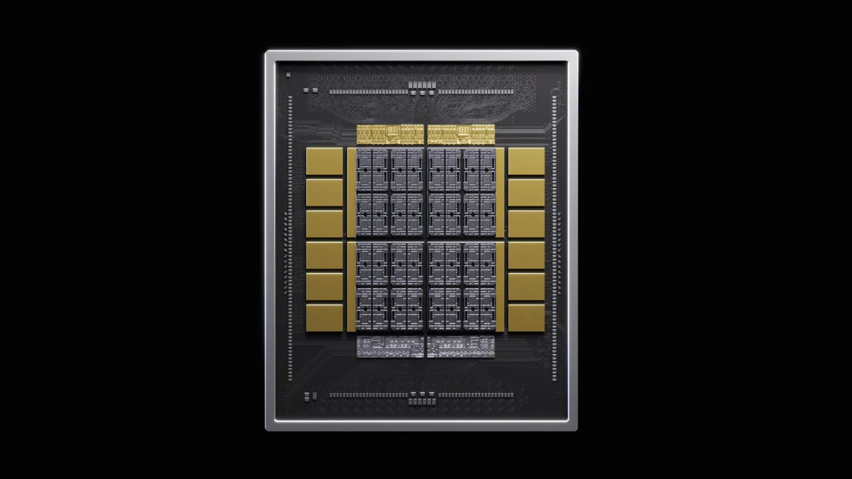
NVIDIA has officially introduced NVHBM, a proprietary High Bandwidth Memory (HBM) architecture designed to fundamentally alter how data is transferred between memory and processing units in next-generation artificial intelligence accelerators. Developed in strategic collaboration with Amazon’s Annapurna Labs, NVHBM represents a significant departure from industry-standard memory configurations by integrating the memory controller directly into the HBM base die. This architectural shift is positioned as a critical solution to the "memory wall"—the growing performance gap between the processing speed of AI chips and the rate at which data can be retrieved from memory. As the industry transitions into the era of trillion-parameter models and agentic AI, NVHBM aims to provide the necessary throughput and power efficiency to sustain the next decade of computational growth.
The Evolution of AI Memory Architecture: From Standard HBM to NVHBM
To understand the significance of NVHBM, it is necessary to examine the current state of High Bandwidth Memory. Traditionally, an XPU—a general term for specialized processing units like GPUs or AI accelerators—contains a memory controller within its own logic die. This controller communicates with external HBM stacks via a physical interface (PHY). While effective for previous generations of hardware, this layout creates physical and thermal constraints. As AI models scale, the amount of area on the silicon dedicated to memory interfaces has increased, leaving less room for the actual compute cores that perform mathematical operations.
NVIDIA’s NVHBM addresses this by utilizing a concept known as NVLink Fusion. By moving the memory controller off the main XPU and embedding it within the base die of the HBM stack itself, NVIDIA has effectively streamlined the communication path. This "custom HBM" approach allows for a narrower physical interface between the processor and the memory, which in turn simplifies the complex routing required on the silicon interposer. According to NVIDIA’s technical documentation, this design reduces the PHY and support area by up to 67%, liberating valuable silicon real estate for additional compute capabilities.
Quantifying the Performance: Bandwidth, Power, and Area Gains
The shift to NVHBM is not merely an architectural curiosity; it delivers measurable improvements across three primary metrics: bandwidth, energy efficiency, and silicon density. NVIDIA has released data comparing NVHBM to the upcoming JEDEC HBM4e standard, which was previously expected to be the high-water mark for memory performance in the late 2020s.
The most immediate benefit is a 30% increase in memory bandwidth compared to standard HBM4e solutions. In the context of Large Language Models (LLMs), bandwidth is often the primary bottleneck during the "inference" phase, where the model generates responses. Higher bandwidth allows the system to feed data to the processing cores faster, reducing latency and increasing the number of tokens generated per second.

Furthermore, NVHBM is projected to reduce power consumption by approximately 15%. In massive data centers housing tens of thousands of GPUs, a 15% reduction in memory power translates to megawatts of saved energy and significantly lower cooling requirements. This efficiency is achieved by shortening the physical distance data must travel and optimizing the signaling between the controller and the DRAM layers.
Finally, by offloading the memory controller, NVIDIA claims that chip designers can reclaim up to 25% of the die area on the main XPU. This allows for the integration of more Tensor Cores, larger caches, or specialized engines for physical AI and robotics, effectively increasing the "compute density" of each chip without increasing its physical footprint.
Strategic Partnership with Amazon’s Annapurna Labs
The development of NVHBM is a collaborative effort involving Amazon’s Annapurna Labs, the specialized silicon design arm of Amazon Web Services (AWS). Annapurna Labs has a long history of developing custom chips, such as the Graviton CPUs and Trainium AI accelerators, which allow AWS to offer high-performance cloud services while maintaining control over the underlying hardware stack.
The partnership focuses on integrating NVHBM technology with the NVLink scale-up architecture. Nafea Bshara, Vice President of Annapurna Labs, noted that the collaboration is intended to benefit future AWS infrastructure designs, specifically pointing toward the next generation of AWS Trainium chips. Starting with Trainium4, Amazon intends to use NVLink Fusion to create a unified rack-scale architecture where NVIDIA GPUs and Amazon’s custom AI chips can coexist and communicate with unprecedented efficiency.
This move signals a shift in the cloud provider landscape. Rather than simply purchasing off-the-shelf components, major hyperscalers like Amazon are working at the silicon level with NVIDIA to co-design the future of the data center. This ensures that the memory architecture is perfectly tuned for the specific workloads—such as agentic AI and autonomous systems—that AWS customers are increasingly demanding.
Addressing the Trillion-Parameter Era and the Memory Wall
The industry’s push toward custom memory solutions is driven by a harsh reality often referred to as the "AI Memory Wall." Data compiled by various research firms, including Micron and SK Hynix, suggests that while AI compute performance has been doubling roughly every six to nine months, memory bandwidth has historically grown at a much slower pace. Every two years, compute capabilities tend to outrun HBM bandwidth by a factor of three.

As models like GPT-4, Llama 3, and their successors move into the trillion-parameter range, the sheer volume of data that must be moved in and out of memory is staggering. Standard HBM architectures are reaching the limits of what can be achieved through traditional scaling. By adopting a custom approach like NVHBM, NVIDIA is attempting to reset the clock on this bottleneck.
The timing of this announcement aligns with NVIDIA’s long-term roadmap. The company has already teased its future "Feynman" GPU architecture, which is expected to launch around 2028. Feynman is slated to be the first major platform to fully adopt NVHBM and 3D die-stacking technologies. Between now and then, the industry will see the rollout of Blackwell Ultra (2025) and Rubin (2026), which will utilize HBM3e and HBM4 respectively, serving as the evolutionary bridge to the custom NVHBM era.
The Competitive Landscape: Samsung, SK Hynix, and Micron
NVIDIA is not the only player exploring the integration of logic into memory dies. The "Big Three" memory manufacturers—Samsung, SK Hynix, and Micron—have all signaled that the transition from HBM3e to HBM4 will involve a fundamental change in how base dies are manufactured.
In previous generations, the base die of an HBM stack was a relatively simple interface. For HBM4, the industry is moving toward "Logic Base Dies." Samsung has indicated it may use its advanced 2nm and 4nm process nodes to manufacture these base dies, effectively turning the bottom of the memory stack into a high-performance processor in its own right. Similarly, SK Hynix has partnered with TSMC to optimize the integration of HBM4 with advanced logic processes.
What sets NVHBM apart is the proprietary nature of the implementation. By establishing its own standard and providing it to multiple memory providers, NVIDIA is creating a controlled ecosystem. This reduces the engineering effort required to qualify memory from different suppliers, as they will all be building to NVIDIA’s specific NVHBM controller specifications. This "standardized custom" approach allows NVIDIA to maintain its performance lead while ensuring a stable supply chain from multiple vendors.
Implications for Agentic and Physical AI
The announcement specifically highlighted "Agentic and Physical AI" as the primary beneficiaries of NVHBM. Agentic AI refers to systems that do not just process text or images but can autonomously perform multi-step tasks, reason through problems, and interact with software tools. These workloads require extremely low latency and high "context window" management, both of which are heavily dependent on memory performance.

Physical AI, which includes robotics and autonomous vehicles, requires the processing of massive amounts of sensor data in real-time. The 25% die area savings offered by NVHBM could be used to integrate specialized hardware for spatial computing or real-time physics simulations directly onto the XPU. By reducing the power consumption of the memory, NVIDIA also makes it more feasible to deploy these high-performance chips in "edge" environments, such as autonomous delivery robots or factory automation systems, where power budgets are tighter than in a liquid-cooled data center.
Conclusion and Future Outlook
The introduction of NVHBM marks the beginning of a new chapter in the semiconductor industry, where the line between "processor" and "memory" continues to blur. By embedding the memory controller into the HBM stack and co-designing the solution with a major cloud partner like Amazon, NVIDIA is reinforcing its "full-stack" approach to AI computing.
As the industry looks toward the 2028 launch of the Feynman architecture, the success of NVHBM will likely be measured by how effectively it enables the next generation of AI models to break through current performance ceilings. With 30% more bandwidth and 15% lower power, NVHBM provides a clear path forward for the trillion-parameter era, ensuring that the silicon of the future is not held back by the memory architectures of the past. The collaboration with Annapurna Labs further suggests that the future of AI will be defined by deep vertical integration, from the memory cells themselves to the rack-scale infrastructure of the world’s largest data centers.