 admin
admin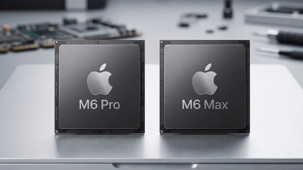
The Evolution of Apple’s Fusion Architecture
At the heart of Apple’s next-generation silicon strategy is the refinement of its "Fusion Architecture," a term the company uses to describe its proprietary approach to chip design and interconnection. According to recent disclosures from the Commercial Times, the base M6 chip is expected to continue utilizing TSMC’s System on Integrated Chips (SoIC-MH) technology. This technology, which was initially introduced with the M5 Pro and M5 Max series, allows for the vertical stacking of chips, significantly reducing the physical footprint of the SoC while enhancing data transfer speeds between components.
However, the upcoming M6 Pro and M6 Max—or potentially their successors in the M7 lineup—are slated to incorporate an even more advanced packaging methodology known as Wafer-Level Multi-Chip Module (WMCM). This transition represents a fundamental departure from the traditional monolithic die design, where all components are fabricated on a single piece of silicon. By moving to a modular WMCM approach, Apple can integrate various "chiplets" fabricated on different process nodes or optimized for specific tasks into a single package. This modularity is expected to integrate logic chips, high-speed LPDDR memory, and I/O controllers with unprecedented interconnect density, effectively eliminating the bottlenecks associated with traditional circuit board traces.
Strategic Shift Toward Modular Design and Yield Optimization
The decision to move away from large monolithic dies is driven by both economic and technical imperatives. As semiconductor manufacturing pushes toward the 2nm and 1.4nm limits, the cost of producing large, complex chips on a single die increases exponentially. Furthermore, the "yield"—the percentage of functional chips per wafer—typically drops as die size increases, because a single microscopic defect can render an entire large chip useless.
By adopting WMCM and SoIC-MH technologies, Apple can manufacture smaller, more reliable chiplets and then assemble them into a larger, more powerful module. This approach offers several key advantages:
- Manufacturing Efficiency: Smaller dies have higher yields, reducing waste and lowering the overall cost per unit.
- Thermal Management: Distributing heat-generating components across a multi-chip module can prevent the thermal throttling issues often found in compact devices like the MacBook Air and iPad Pro.
- Power Efficiency: Shorter interconnects between logic and memory reduce the energy required to move data, a critical factor for extending the battery life of mobile devices.
- Scalability: Apple can more easily scale performance by adding more logic chiplets to a package, allowing for a more streamlined transition between the "Pro," "Max," and "Ultra" tiers of its silicon.
TSMC’s Role and the Expansion of Packaging Capacity
Apple’s ambitious roadmap is inextricably linked to its partnership with Taiwan Semiconductor Manufacturing Company (TSMC). As the sole foundry for Apple Silicon, TSMC has been aggressively expanding its advanced packaging facilities to meet the anticipated demand for WMCM and SoIC technologies. Industry projections indicate a massive scaling of production capacity over the next twenty-four months.
According to the latest manufacturing data, TSMC’s monthly WMCM capacity is projected to reach approximately 60,000 wafers by the end of 2026. This capacity is expected to double, exceeding 120,000 wafers per month, by 2027. This expansion is particularly noteworthy given the current global surge in demand for Artificial Intelligence (AI) accelerators from companies like Nvidia and AMD, which has strained TSMC’s CoWoS (Chip on Wafer on Substrate) production lines. Despite this "AI boom," Apple’s position as TSMC’s most lucrative and consistent customer ensures it receives priority access to these next-generation packaging lines. Analysts suggest that Apple’s shift to WMCM will not only benefit its Mac and iPad lines but will also serve as a blueprint for its future AI-focused data center chips.
The A20 Pro and the iPhone 18 Connection
While the M-series chips represent the pinnacle of Apple’s computing performance, the packaging innovations are expected to debut in the mobile space. The A20 Pro chipset, which will power the upcoming iPhone 18 Pro, iPhone 18 Pro Max, and the highly anticipated "iPhone Fold," is rumored to be the first commercial application of the refined WMCM technology.

The integration of WMCM in the iPhone 18 series is intended to address the increasing memory demands of on-device AI. As Apple Intelligence—the company’s suite of generative AI features—becomes more complex, the need for high-bandwidth memory access becomes paramount. By using WMCM to bring LPDDR memory closer to the A20 Pro’s neural engine, Apple can achieve the low-latency performance required for real-time language processing and image generation without significantly increasing power consumption.
The M6 vs. M7 Controversy: A Timeline of Predictions
There remains a degree of conflicting information regarding the naming convention and release schedule of Apple’s high-end silicon. Renowned Bloomberg analyst Mark Gurman has previously suggested that Apple might skip the M6 Pro and M6 Max entirely. In this scenario, Apple would focus its engineering resources on the M7 series, which is reportedly being designed from the ground up to prioritize AI operations and "on-device intelligence."
The proposed timeline for these developments is as follows:
- H1 2026: Launch of the base M7 SoC. This chip is expected to feature a unified memory bandwidth of 240GB/s, representing a 56 percent increase over the projected bandwidth of the M5 series.
- Late 2026: Introduction of the A20 Pro with WMCM technology in the iPhone 18 lineup.
- 2027: Expansion of WMCM to the M7 Pro and M7 Max, coinciding with TSMC’s capacity peak.
- Beyond 2027: Development of the M8 series, which is rumored to focus on even more advanced 2nm or sub-2nm process nodes.
The discrepancy between the Commercial Times report (which claims M6 Pro/Max development is ongoing) and Gurman’s predictions (which favor an M7 transition) may simply be a matter of internal nomenclature. It is possible that the technology originally slated for the M6 Pro/Max has been re-branded or folded into the M7 development cycle to align with Apple’s marketing focus on AI.
Market Implications and Competitive Analysis
Apple’s aggressive pursuit of advanced packaging places it in a unique position within the personal computing market. While competitors like Intel (with its Meteor Lake and Lunar Lake architectures) and AMD (with its Ryzen 9000 series) have also embraced chiplet-based designs, Apple’s vertical integration allows it to optimize the software-hardware stack in ways that its rivals cannot easily replicate.
Industry observers note that the move to 240GB/s bandwidth on a base-level chip would effectively place Apple’s entry-level MacBooks in a performance bracket previously reserved for high-end workstations. This has significant implications for professional workflows in video editing, 3D rendering, and software development. Furthermore, by securing TSMC’s packaging capacity, Apple creates a high barrier to entry for other consumer electronics manufacturers who may wish to adopt similar modular designs but find themselves "queued" behind Apple and the major AI chip providers.
Conclusion: The Future of Apple Silicon
The shift toward SoIC-MH and WMCM technologies marks the beginning of a new era for Apple Silicon—one defined by modularity, interconnect density, and AI-first architecture. Whether these innovations arrive under the M6 or M7 banner, the objective remains clear: to break the physical constraints of monolithic silicon and deliver performance gains that outpace traditional Moore’s Law scaling.
As TSMC continues to ramp up its facilities in Taiwan and potentially its new sites in Arizona and Japan, the global supply chain will be watching closely. The success of the A20 Pro and the subsequent M-series chips will determine whether Apple can maintain its dominance in the premium device market or if the complexities of modular manufacturing will present unforeseen challenges. For now, the data points toward a future where the distinction between a "mobile chip" and a "computer chip" continues to blur, driven by a shared foundation of advanced, wafer-level packaging.