
The fundamental limitation of modern computing has long been dictated not by logic or software, but by the physical properties of heat. For decades, the electronics industry has operated under a rigid thermal ceiling; most silicon-based semiconductors and memory storage devices begin to fail or suffer permanent structural damage when temperatures exceed approximately 200 degrees Celsius. This threshold has restricted the deployment of advanced computing in the world’s most extreme environments, from the crushing heat of the Venusian surface to the interior of nuclear reactors and deep-earth geothermal wells. However, a research team at the University of Southern California (USC) has recently announced a significant technological leap that effectively shatters this barrier, demonstrating a memory device capable of functioning at temperatures as high as 700 degrees Celsius.
The study, led by Professor Joshua Yang of the USC Viterbi School of Engineering and published in the journal Science, introduces a specialized memristor—a nanoscale electronic component that serves as both a storage medium and a processor. The device not only survived 700 degrees Celsius—a temperature exceeding the melting point of lead and the surface heat of Venus—but it also maintained operational integrity without showing signs of degradation. According to the research team, 700 degrees was simply the upper limit of their testing equipment, suggesting the device’s actual thermal tolerance may be even higher.
The Architecture of Extreme Heat Resistance
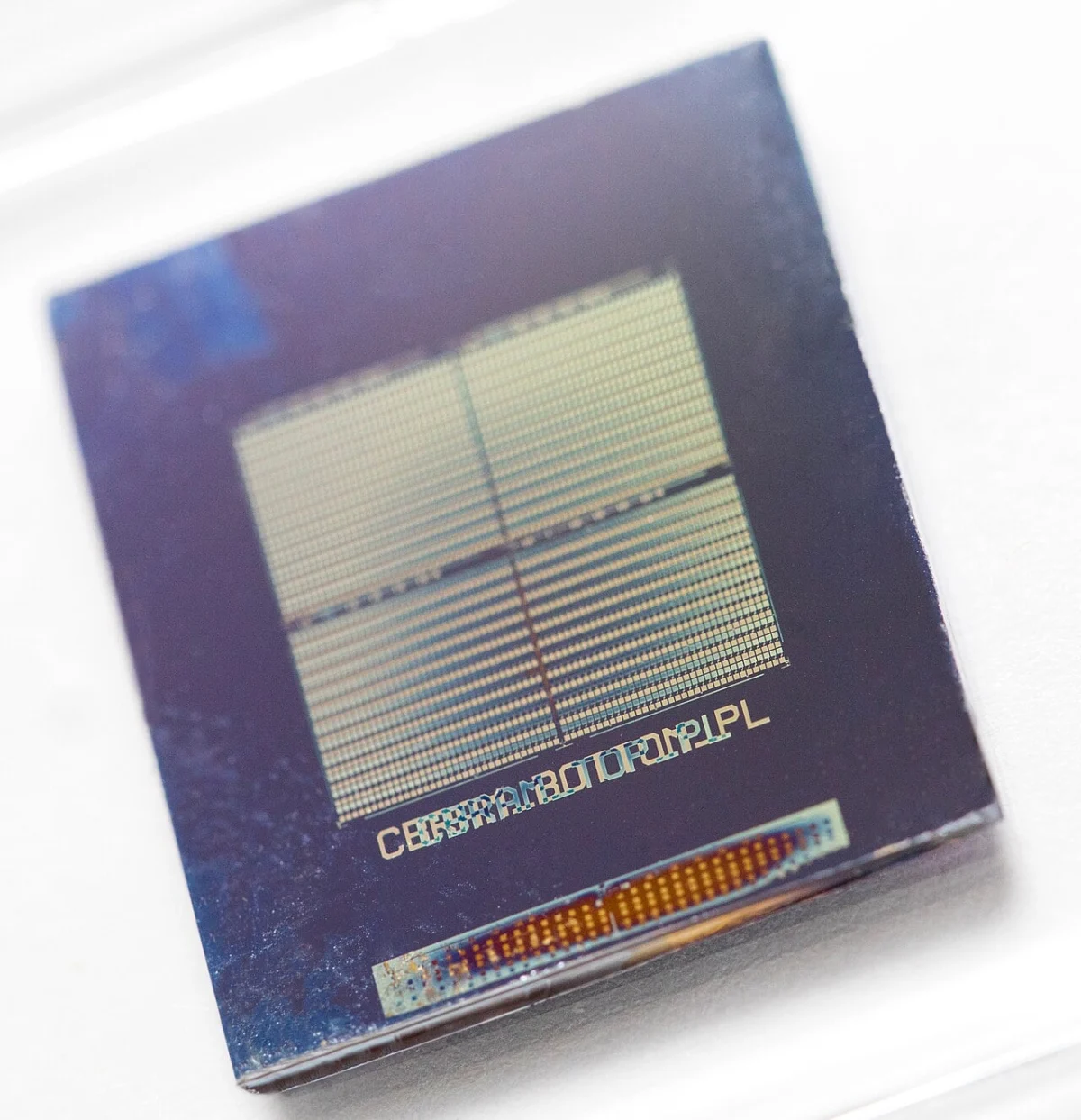
The breakthrough lies in a sophisticated "sandwich" architecture of advanced materials, each chosen for their extreme thermal stability. At the core of the device is a ceramic layer of hafnium oxide, a material already familiar to the semiconductor industry for its high-k dielectric properties. This is flanked by electrodes made of tungsten, the chemical element with the highest melting point of any known metal (3,422 degrees Celsius).
While the combination of tungsten and hafnium oxide provided a sturdy foundation, the critical innovation was the inclusion of an atomically thin layer of graphene. In standard electronic components, extreme heat causes metal atoms from the electrodes to migrate into the insulating layers. This process, known as diffusion or electromigration, eventually creates a metallic bridge between the electrodes, causing a short circuit that permanently destroys the chip.
The USC team discovered that placing graphene between the tungsten and the hafnium oxide created an impenetrable barrier. Professor Yang described the relationship between the tungsten and graphene as being chemically similar to "oil and water." The tungsten atoms, despite the kinetic energy provided by the 700-degree environment, are unable to take hold or anchor onto the graphene surface. This lack of chemical affinity prevents the formation of the metallic filaments that typically lead to device failure, allowing the memristor to switch between "on" and "off" states reliably despite the thermal agitation.
A Discovery Rooted in Serendipity
The path to this discovery was not a linear pursuit of heat resistance. The research team was originally investigating an entirely different set of properties for a new type of computing component when they encountered the anomalous stability of the graphene-tungsten interface. Upon realizing the implications of their findings, the team utilized advanced electron microscopy to observe the device at the atomic level and employed quantum-level computer simulations to verify the underlying physics.

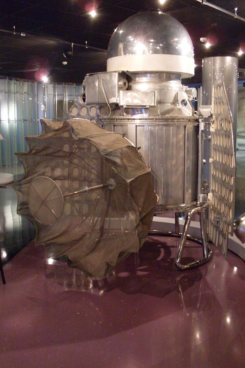
This accidental discovery addresses a problem that has plagued aerospace and energy engineering for over half a century. In the history of space exploration, the Soviet Union’s Venera missions to Venus provide a stark example of the limitations of conventional electronics. Despite being heavily shielded and cooled, the most successful landers survived for less than two hours before the 460-degree Celsius surface temperature fried their internal circuitry. The USC breakthrough suggests a future where landers could operate on the Venusian surface for months or even years, performing complex data analysis without the need for massive, heavy cooling systems.
Comparative Data and Technical Performance
To understand the magnitude of this achievement, it is necessary to compare the USC memristor to current industry standards. Standard consumer-grade electronics are rated for "Commercial" temperatures (0°C to 70°C) or "Industrial" temperatures (-40°C to 85°C). Specialized "Automotive Grade" or "Military Grade" components can occasionally reach 125°C to 150°C.
The USC device’s performance at 700°C represents a nearly fourfold increase over the most robust specialized electronics currently in use. During testing, the researchers subjected the device to repeated "write" and "read" cycles—the process of storing and retrieving data—at these elevated temperatures. The data remained stable, and the switching mechanism remained precise. This stability is vital for "non-volatile" memory, which must retain information even when the power is turned off, a task that becomes exponentially more difficult as heat increases the likelihood of data corruption.
Industry and Scientific Reactions
The announcement has garnered significant attention from both the scientific community and industrial sectors that operate in high-temperature environments. While official statements from agencies like NASA or the Department of Energy are typically reserved for later stages of commercial development, the implications for their respective fields are clear.
Aerospace engineers have long sought "high-T" (high temperature) electronics to reduce the weight of spacecraft. Currently, a significant portion of a probe’s mass is dedicated to thermal protection systems (TPS) and active cooling loops. If the control computers and sensors can survive the ambient heat of a planet or the proximity to a rocket engine, those cooling systems can be downsized or eliminated, allowing for more scientific instrumentation or longer mission durations.
In the energy sector, the demand is equally high. Geothermal energy involves drilling several kilometers into the Earth’s crust, where temperatures can exceed 300 degrees Celsius. Current sensors used in "Measurement While Drilling" (MWD) operations often fail, leading to expensive delays. Similarly, in the nuclear power industry, sensors that can operate inside or near a reactor core without failing due to heat or radiation would provide a new level of safety and operational monitoring.
Implications for the Future of Computing
Beyond simply surviving heat, the use of memristors suggests a shift in how we think about computing architecture. Memristors are a key component in "neuromorphic computing," a field that seeks to mimic the efficiency of the human brain. By combining memory and processing into a single nanoscale structure, these devices can process information with a fraction of the energy required by traditional silicon chips.
The fact that this efficiency can now be achieved in extreme environments opens new frontiers for Artificial Intelligence. We may see the development of "edge computing" in locations previously thought impossible—autonomous drones monitoring forest fires from within the smoke plumes, or smart sensors embedded directly into the ceramic linings of jet engines to provide real-time diagnostic data.
Timeline and Path to Commercialization
While the laboratory results are a landmark achievement, the transition from a "lab bench" prototype to a mass-produced commercial chip involves several critical steps:
- 2024-2025: Material Scaling: The research team will likely focus on scaling the fabrication process. While a single memristor is a breakthrough, a functional computer chip requires millions or billions of these components integrated onto a single substrate.
- 2026-2027: Reliability Testing: Long-term "stress tests" will be required to see if the device can survive 700-degree heat for years rather than hours or days.
- 2028 and Beyond: Integration: Collaboration with semiconductor foundries will be necessary to integrate these tungsten-graphene-ceramic structures into existing manufacturing pipelines.
Professor Yang has acknowledged that the road to a finished product is long, but he maintains that the most difficult hurdle—the physical impossibility of the task—has been cleared. The "missing component" for high-temperature computing has been identified and proven.
Conclusion
The development of the 700-degree Celsius memory chip at the University of Southern California marks the end of the "200-degree ceiling" that has defined the semiconductor era. By leveraging the unique atomic properties of graphene and the thermal resilience of tungsten, the team has created a device that thrives where all others perish.
This discovery does more than just improve existing technology; it expands the map of where human intelligence, via our machines, can go. Whether it is the exploration of the solar system’s most hostile planets or the optimization of clean energy production deep beneath the Earth’s surface, the USC memristor provides the cognitive foundation for the next generation of extreme-environment engineering. As the destination is now clearly in sight, the focus shifts from asking "if" we can compute in the heat, to asking "what" we will discover once we are there.