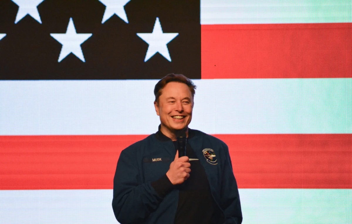
Austin, Texas – Elon Musk, the enigmatic entrepreneur at the helm of Tesla, SpaceX, and XAI, has announced a monumental undertaking: the construction of a "Terafab" facility dedicated to manufacturing custom artificial intelligence (AI) chips. The audacious plan, shared at an event in downtown Austin on Saturday night, aims to address what Musk perceives as a critical bottleneck in the global semiconductor supply chain, which he claims is hindering the rapid advancement of his various ventures in AI and robotics. The proposed facility is slated to be built near Tesla’s sprawling Austin headquarters and Gigafactory, integrating seamlessly with the company’s burgeoning presence in the region.
Musk articulated the necessity of this venture with characteristic directness: "We either build the Terafab or we don’t have the chips, and we need the chips, so we build the Terafab." This statement underscores a strategic imperative driven by the insatiable demand for high-performance computing components essential for developing sophisticated AI models, powering autonomous vehicles, and enabling advanced robotics. The envisioned Terafab would serve as a crucial internal resource, providing bespoke silicon solutions optimized for the unique requirements of Tesla’s self-driving initiatives and Optimus humanoid robot, SpaceX’s Starlink satellite network and Starship program, and XAI’s pursuit of artificial general intelligence.
The Genesis of Terafab: A Strategic Imperative
The announcement comes at a time when the global semiconductor industry is experiencing unprecedented demand, particularly for AI accelerators. Companies like NVIDIA have seen their market capitalization surge, reflecting the critical role their Graphics Processing Units (GPUs) play in the AI revolution. However, this demand has also led to supply constraints, extended lead times, and significant cost pressures, especially for companies pushing the boundaries of AI research and deployment. For Musk’s ecosystem, which operates on aggressive timelines and requires highly specialized, energy-efficient chips, reliance on external suppliers presents both a strategic vulnerability and a potential brake on innovation.
Tesla, in particular, has a history of developing custom silicon. Its "Dojo" supercomputer project, designed to train its neural networks for Full Self-Driving (FSD) capabilities, already incorporates custom-designed D1 chips. While Dojo has made progress, its ramp-up has reportedly faced challenges, highlighting the complexities of both designing and deploying cutting-edge AI hardware. By taking chip manufacturing in-house, Musk aims to achieve greater control over the design-to-production cycle, allowing for rapid iteration, tighter integration between hardware and software, and potentially significant cost savings in the long run. This move is reminiscent of Apple’s successful transition to custom ARM-based processors for its Mac lineup, which granted it greater performance, power efficiency, and design flexibility.
SpaceX’s needs are equally pressing. The Starlink constellation, already comprising thousands of satellites, requires robust, radiation-hardened processors for on-orbit data processing, beamforming, and inter-satellite communication. As the Starship program progresses towards interplanetary missions, the need for autonomous systems and high-bandwidth data processing in hostile environments will only intensify. The Terafab could provide specialized chips that meet these stringent space-grade requirements, which are often not priorities for commercial foundries focused on consumer electronics.
Scaling the Summit: Unprecedented Computing Ambitions
Musk’s stated goals for the Terafab are nothing short of monumental. He outlined an ambition to manufacture chips capable of supporting 100 to 200 gigawatts (GW) of computing power per year on Earth, alongside an astounding one terawatt (TW) in space. To put these figures into perspective, a large-scale modern data center might consume tens to a few hundred megawatts (MW) of power. A gigawatt is 1,000 megawatts, and a terawatt is 1,000 gigawatts. Achieving 100-200 GW of new computing capacity annually on Earth, and especially 1 TW in space, represents a staggering leap beyond current capabilities and infrastructure.
The terrestrial goal implies a massive influx of processing power, potentially fueling dozens of hyperscale AI data centers or an exponential increase in edge computing devices. The space-based target, however, is truly visionary. A terawatt of computing in orbit would necessitate an entirely new paradigm for space infrastructure. It would require colossal advancements in orbital power generation (likely massive solar arrays), ultra-efficient cooling systems capable of dissipating immense heat in a vacuum, and launch capabilities far exceeding even Starship’s projected capacity to deliver the sheer volume and mass of hardware into orbit. This hints at Musk’s long-term vision for orbital data centers, potentially leveraging the vacuum and extreme cold of space for enhanced efficiency, or even for applications requiring ultra-low latency processing near celestial bodies. Such a facility could be transformative for scientific research, remote sensing, and even future space colonization efforts, enabling unprecedented data processing capabilities far from Earth’s gravitational well.
The Semiconductor Industry Landscape: A Formidable Challenge
Musk’s foray into semiconductor manufacturing is an entry into one of the world’s most complex, capital-intensive, and technologically demanding industries. The global semiconductor market is dominated by a few highly specialized players: TSMC (Taiwan Semiconductor Manufacturing Company) and Samsung Foundry are the leading contract manufacturers (foundries) producing the most advanced chips for companies like Apple, NVIDIA, and AMD. Intel, while a major designer and manufacturer, primarily serves its own needs and is only recently making a concerted effort to become a leading foundry for external customers.
Building a state-of-the-art semiconductor fabrication plant (fab) is an undertaking that typically costs tens of billions of dollars. The most advanced facilities, utilizing Extreme Ultraviolet (EUV) lithography machines from ASML (each costing hundreds of millions of dollars), require years of planning, construction, and commissioning – often five to ten years from groundbreaking to full production. The process involves thousands of highly specialized steps, requiring an army of materials scientists, electrical engineers, physicists, and chemical engineers. The supply chain for raw materials, chemicals, and precision equipment spans the globe, making it susceptible to geopolitical shifts and disruptions.
As Bloomberg noted, Musk does not have a background in semiconductor manufacturing. While he has a proven track record of attracting top talent and disrupting established industries (automotive, aerospace), the deep institutional knowledge and intricate ecosystem required for leading-edge chip production represent a unique challenge. Recruiting the necessary highly specialized workforce in an already tight global talent market will be a significant hurdle. Furthermore, achieving economies of scale and competitive yields – the percentage of functional chips produced from a wafer – requires years of optimization and continuous innovation.
Location and Integration: Austin’s Expanding Tech Hub
The choice of Austin, Texas, as the site for the Terafab is strategically sound. Tesla’s Gigafactory Texas, a colossal manufacturing complex, is already a hub for vehicle production and battery development. Proximity to this existing infrastructure could offer synergies in terms of power supply, logistics, and potentially a shared talent pool, particularly for engineers accustomed to large-scale manufacturing challenges. Austin itself has emerged as a significant tech hub, attracting talent and investment, which could aid in recruitment efforts. The potential economic impact of such a massive facility on the Austin region would be substantial, creating thousands of high-paying jobs and further solidifying the city’s reputation as a burgeoning innovation center. However, local infrastructure, particularly water and electricity supply, would need to be significantly augmented to support a fab of this projected scale.
Historical Context and Feasibility: The Musk Factor
Assessing the Terafab announcement requires a balanced perspective, acknowledging Elon Musk’s unique history of both extraordinary achievement and ambitious, often delayed, promises. On one hand, companies like Tesla and SpaceX have defied conventional wisdom, revolutionizing their respective industries through audacious goals and relentless execution. SpaceX’s reusable rockets and Starlink satellite internet constellation, and Tesla’s dominance in electric vehicles, stand as testaments to Musk’s ability to turn seemingly impossible visions into reality.
On the other hand, Musk has a well-documented history of setting highly aggressive timelines and goals that are not always met within the initial projections. Examples include the prolonged ramp-up of Cybertruck production, the perpetually "next year" promise of full self-driving capability, and the challenges faced in scaling the Dojo supercomputer. The original article cites instances of Musk "overpromising on goals and timelines," a pattern that industry analysts and investors often consider when evaluating his new announcements. This pattern does not necessarily invalidate the vision but suggests that the path to realizing the Terafab will likely be fraught with unexpected challenges and potentially significant delays beyond any initial, unspoken timeline. The sheer scale and complexity of advanced semiconductor manufacturing make it particularly vulnerable to such optimistic scheduling.
Industry Reactions and Expert Analysis
While no official statements from major semiconductor players have been released, industry experts and analysts are likely to view Musk’s announcement with a mix of intrigue, skepticism, and perhaps a touch of apprehension. Established foundries like TSMC and Samsung might privately express skepticism regarding the feasibility of a newcomer quickly achieving leading-edge production capabilities, given the immense intellectual property, operational experience, and capital required. However, they might also recognize the underlying demand that Musk is attempting to address, potentially spurring further investment in their own capacity expansion.
Analysts will undoubtedly point to the astronomical capital expenditure (CapEx) required, easily estimated in the tens of billions of dollars for a single advanced fab, let alone multiple facilities implied by the "Terafab" moniker. They will also highlight the years-long timeline for construction and qualification, suggesting that even if successful, the Terafab would not alleviate immediate chip shortages for Tesla or SpaceX. Furthermore, the risk of diverting significant financial and human resources from Tesla and SpaceX’s core businesses, which themselves are incredibly capital-intensive, will be a major point of concern. Some might argue that a more pragmatic approach would be to heavily invest in partnerships with existing foundries to secure dedicated capacity, rather than attempting to build a competing ecosystem from scratch.
Governments, particularly those focused on semiconductor sovereignty, might view Musk’s initiative with interest. The global push for domestic chip manufacturing, spurred by geopolitical tensions and supply chain vulnerabilities, could see governments eager to support such a large-scale project, potentially through subsidies or incentives, especially if it promises to create a significant number of high-tech jobs and reduce reliance on overseas manufacturing.
Implications for Tesla, SpaceX, and the AI Ecosystem
If successful, the Terafab initiative could have profound implications across Musk’s empire and potentially the broader tech landscape.
- Strategic Autonomy: The most immediate benefit would be a dramatic reduction in reliance on external chip suppliers. This would grant Tesla, SpaceX, and XAI unparalleled control over their hardware roadmap, intellectual property, and supply chain, minimizing exposure to geopolitical risks, trade disputes, and market fluctuations.
- Performance Optimization: In-house chip design and manufacturing would allow for extreme optimization of silicon for specific AI workloads, robotics control, and space applications. This tailored hardware could provide a significant performance and efficiency advantage over general-purpose chips, accelerating the development of FSD, Optimus, and advanced AI models.
- Cost Efficiency: While the initial investment would be colossal, long-term internal production could lead to significant cost savings per chip, especially as volumes scale. This would positively impact the profitability of Tesla vehicles and the operational costs of Starlink and future SpaceX missions.
- Competitive Edge: Control over advanced silicon could provide a formidable competitive advantage, enabling innovations that external suppliers might not prioritize or be able to deliver on the required timelines.
- Broader Impact: A fully functional Terafab, especially one achieving the stated computing targets, could potentially disrupt the existing semiconductor foundry model, or at the very least, stimulate further innovation and competition within the industry. It could also set a new precedent for vertical integration in high-tech industries.
However, the risks are equally immense. The project could drain vast amounts of capital and divert critical engineering talent from Tesla and SpaceX’s primary missions. A failure to achieve competitive yields or leading-edge performance could result in billions of dollars in losses and a significant setback for Musk’s ambitions. The technological hurdles are arguably greater than those faced in automotive or aerospace manufacturing, demanding a level of precision and scientific expertise that is globally scarce.
The Road Ahead: Challenges and Opportunities
Elon Musk’s Terafab announcement is a bold declaration of intent, emblematic of his career-long pursuit of audacious, transformative goals. While the lack of a specific timeline leaves much to the imagination, the vision itself is clear: to eliminate external dependencies and accelerate the future of AI and space exploration through self-sufficiency in chip manufacturing.
The path from concept to a functioning Terafab capable of producing hundreds of gigawatts of computing power annually, let alone a terawatt in space, is fraught with immense challenges. It will require not only staggering capital investment but also the successful recruitment of an elite team of semiconductor experts, the mastery of incredibly complex manufacturing processes, and the navigation of a highly competitive and geopolitically sensitive industry.
The world will now watch to see if Musk can once again defy expectations and build a foundational pillar for his technological empire, or if the Terafab will join the list of his more protracted and challenging endeavors. What is certain is that the semiconductor industry, and indeed the broader tech world, has just been put on notice that Elon Musk is serious about controlling his own silicon destiny, no matter how immense the undertaking.